Back to Menu
고대역폭 메모리(HBM)
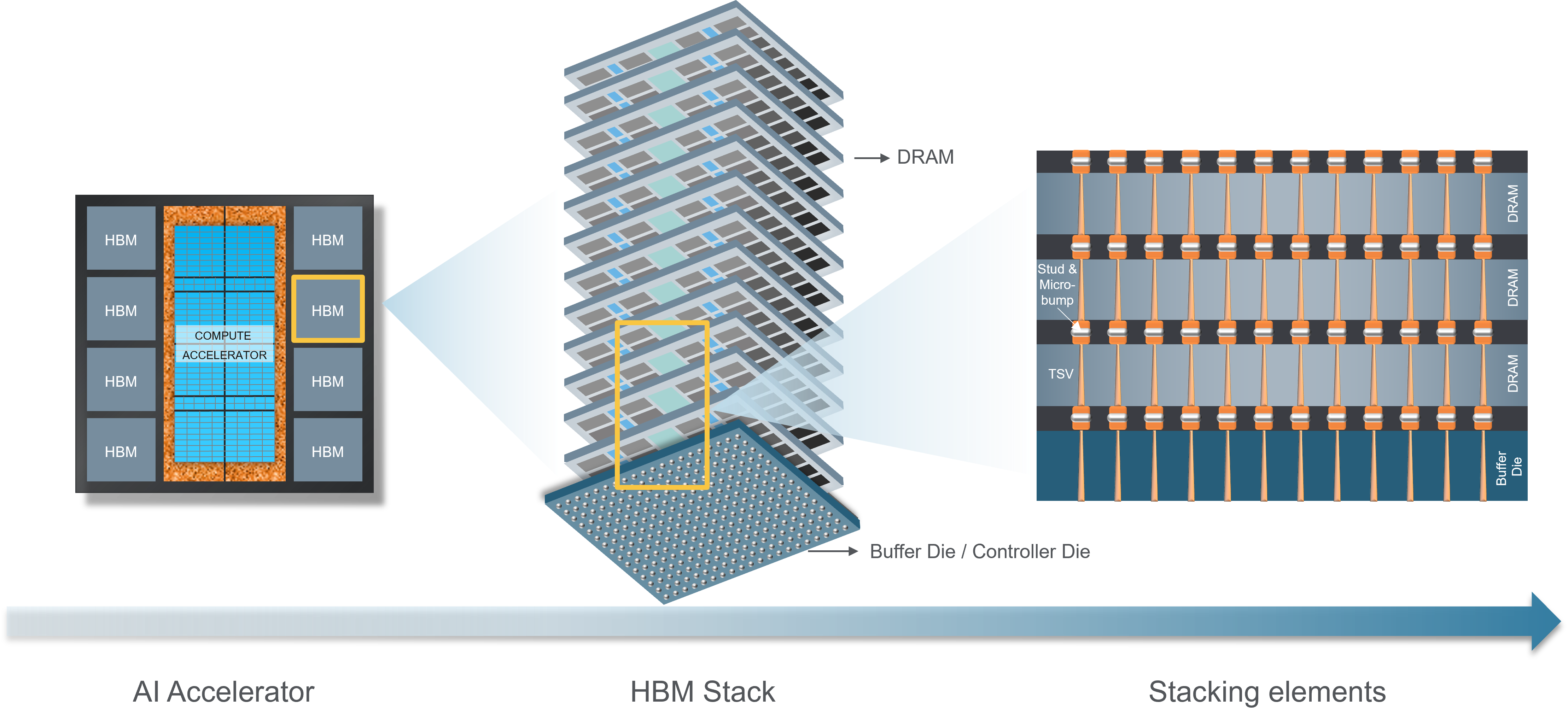
AI 애플리케이션에 필요한 방대한 양의 메모리를 제공하기 위해 칩 제조업체는 고급 DRAM 스택으로 구축된 고성능, 저지연 아키텍처인 고대역폭 메모리(HBM)로 전환했습니다. DRAM 칩의 혁신도 중요하지만, HBM의 밀도와 대역폭은 첨단 3D 패키징을 통해 실현됩니다. 어플라이드 머티어리얼즈® 는 업계의 HBM 도입 증가를 지원하는 데 필요한 재료 공학 기술 분야의 선두주자입니다.
HBM 제조 공정은 웨이퍼의 앞면과 뒷면 양쪽면을 상호 연결 할수 있는 기둥과 실리콘 관통전극(TSV)을 형성하는 등 많은 핵심 재료 엔지니어링 단계를 필요로 합니다.
어플라이드 머티어리얼즈는 더 높은 종횡비의 TSV를 구현하고 비아 트렌치 내에서 더 나은 커버리지를 제공하는 유전체 및 금속 증착 기술을 개발했습니다. 프로듀서™ InVia™ 2 CVD 시스템은 비아 측벽의 형상에 따라 정확하고 균일하게 증착되는 유전체 라이너를 저온 증착하는 데 적합한 공정을 사용합니다. 마찬가지로, 당사의 Endura™ Ventura™ 2 PVD 시스템은 금속 증착 제어를 강화하여 배리어 시드 층을 잘 덮을 수 있도록 하여 전기적 성능과 신뢰성을 높입니다.
TSV 외에도 마이크로 범프 필러는 HBM 스택의 전기 및 열 성능에 매우 중요합니다. 마이크로 범프의 크기와 피치를 모두 줄이는 데 상당한 혁신이 있었지만, 이러한 범프와 해당 본드 패드의 크기가 줄어들면서 접촉 저항은 기하급수적으로 증가합니다. 당사의 고유한 Volaris™ 전세정 기술과 업계 최고의 언더 범프 금속배선용 PVD의 조합은 접촉 저항과 기생 전력을 줄이는 동시에 범프 신뢰성 개선에 도움이 됩니다. 어플라이드 머티어리얼즈의 Nokota™(ECD)와 함께 주요 고객사에서 마이크로 범프 제작을 위한 중요한 위치를 차지하고 있습니다.
HBM 가공의 또 다른 과제는 매우 얇은 웨이퍼 조각을 적층하는 것으로, 웨이퍼 조각 뒤틀림과 휘어짐으로 인해 공정에 지장을 줄 수 있습니다. 당사의 Producer™ Avila™ PECVD 시스템은 웨이퍼 뒷면에 얇은 유전막을 저온에서 증착하여 칩 제조업체가 필름의 응력을 조절하여 뒤틀림을 제어할 수 있도록 합니다.