Products & Technologies
Back to Menu
Products & Technologies
Services
Resources
A High-Performance, Low-Latency Architecture
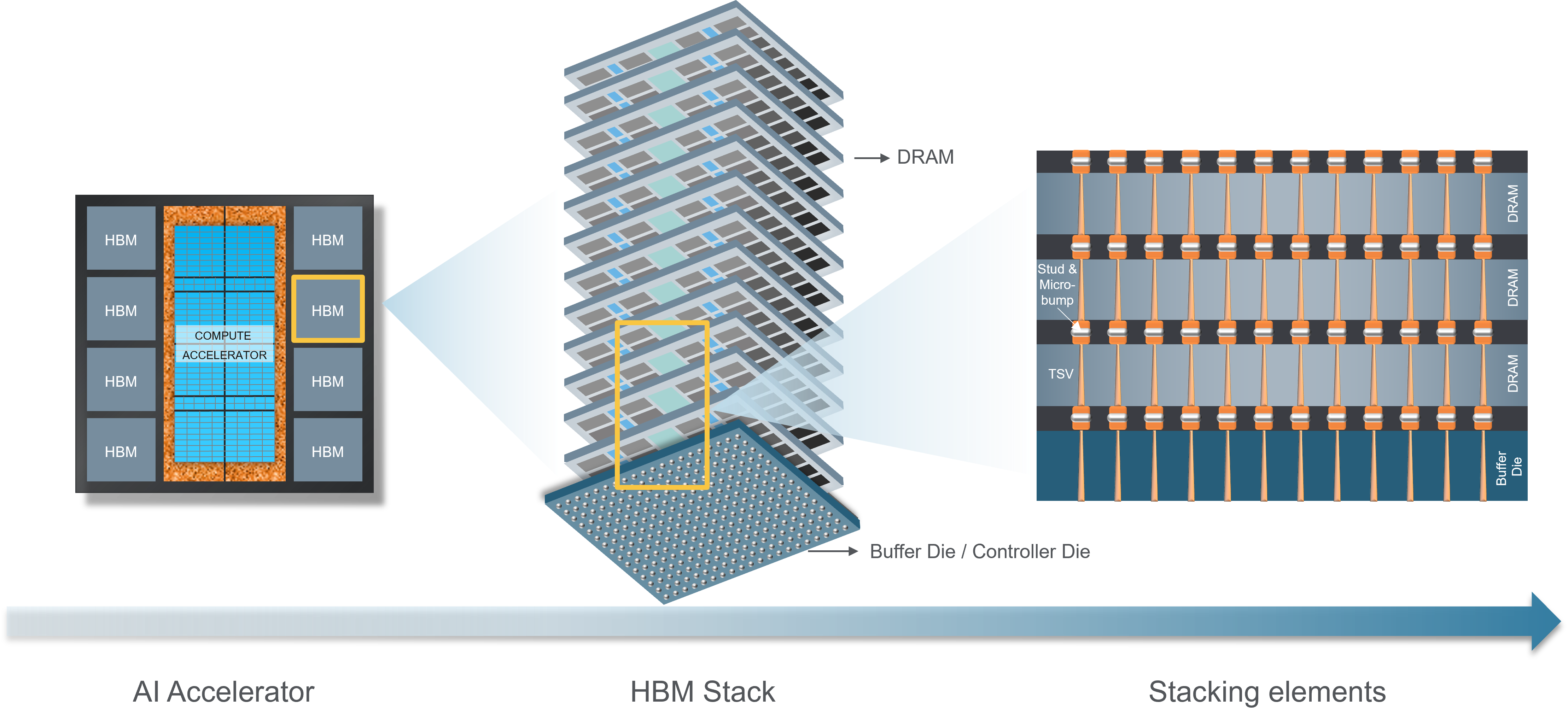
To provide the massive amounts of memory required for AI applications, chipmakers have turned to high-bandwidth memory (HBM) – a high-performance, low-latency architecture built from stacks of advanced DRAM. While innovation in DRAM chips is important, the density and bandwidth behind HBM is realized through advanced 3D packaging. Applied Materials® is a leader in the materials engineering technologies needed to support the industry’s growing adoption of HBM.
The HBM manufacturing flow requires many key materials engineering steps, including the formation of interconnect pillars and through-silicon vias (TSVs) on both the front and back side of the wafer.
Applied Materials has developed dielectric and metal deposition technologies that enable higher-aspect-ratio TSVs and provide better coverage within via trenches. Our Producer™ InVia™ 2 CVD system uses a propriety process that enables low-temperature deposition of a uniform dielectric liner that precisely follows the geometry of the via sidewalls. Similarly, our Endura™ Ventura™ 2 PVD system increases the control of metal deposition to ensure good coverage of the barrier-seed layers, which delivers higher electrical performance and reliability.
Besides TSVs, micro-bump pillars are critical to the electrical and thermal performance of HBM stacks. While there has been significant innovation in reducing both the dimension and pitch of micro-bumps, contact resistance grows exponentially as these bumps and their corresponding bond pads shrink in size. The combination of our unique Volaris™ preclean technology and our industry-leading under-bump metallization PVD helps reduce contact resistance and parasitic power while improving bump reliability. In conjunction with Applied Materials's Nokota™ ECD, we have significant positions for micro-bump fabrication at leading customers.
Another growing challenge with HBM processing is the stacking of very thin dies, which can be impeded by die warpage and bowing. Our Producer™ Avila™ PECVD system deposits a thin dielectric film on the back side of the wafer at low temperature, allowing chipmakers to control warpage by modulating the stress of the film.

