NANOCHIP FAB SOLUTIONS


July 2018 Edition

Leveraging the Digital Twin in Smart Microelectronics Manufacturing

By James Moyne

Among the many tenets of smart manufacturing,[1] “digital twin” solutions represent a significant opportunity for microelectronics manufacturers to leverage existing and emerging technologies to improve quality and throughput, and reduce variability and cost.

The microelectronics industry is working vigorously to leverage the big data revolution and tap into smart manufacturing (SM) and Industry 4.0 strategies. These promise to improve integration and analytical capabilities, and enable solutions such as predictive maintenance and optimized scheduling and dispatch. One key SM tenet receiving considerable attention is the so-called “digital twin.” In this article we examine this concept and illustrate how the microelectronics industry is well-positioned for leadership in its technology development and implementation.

SCIENCE FICTION BECOMES REALITY

The term “digital twin” (DT) invokes thoughts of science fiction: Isaac Asimov; films like 2001 A Space Odyssey and I Robot; and even human cloning. So to many, the vision of a DT in manufacturing implies a computer replica of everything in the factory from components and equipment through systems, and maybe even the actions and behaviors of people. While this may indeed be a future reality, it is important to take a step back, understand how we define digital twin in manufacturing, and then assess how we can leverage this concept today and moving forward.

A generally accepted definition of DT can be found in Wikipedia, namely “A digital twin refers to a digital replica of physical assets, processes and systems that can be used for various purposes.” [2] If we break down this definition, we realize that DT is more than just replicas or models of things (as we see in movies), but also models of processes and systems. For example, in addition to a duplication of the etch system configuration, a model of an etch application process, pump health profile, or product flow at a detailed, or even high level in the fab is considered to be part of the DT family. Assuming this more complete definition of DT we can make the following statements on the state of the art and vision for DT in microelectronics manufacturing:

  • The industry is already successfully employing DT components fab-wide. Applied Materials has been working with customers to realize these DT components in a way that can provide the best customized benefits.
  • The extraordinary scale and precision required to repeatably create microelectronic devices make this kind of manufacturing one of the most intricate and sophisticated in the world, and we have had to develop DT technology to meet our manufacturing needs. As such, our industry is arguably a leader in driving aspects of DT technology advancement.
  • The industry is beginning to explore and benefit from abstracting and combining these DT components.
  • The industry has a realistic vision and roadmap for DT that will provide for significant improvements in quality, throughput and reductions in variability and costs over the next 10 years.

In the remainder of this article each of these points will be explored in detail, along with case studies of DT successes.

DIGITAL TWIN IN TODAY’S FABS

Without realizing it, many fabs today are already at the forefront of the revolution, having pioneered many DT technologies and providing testaments to DT success. Our existing pervasive technologies, such as run-to-run (R2R) control and real-time scheduling and dispatch (S/D), and emerging technologies such as predictive maintenance (PdM) and virtual metrology (VM) are key members of the DT family. This section examines how these technologies are being leveraged in today’s fabs.

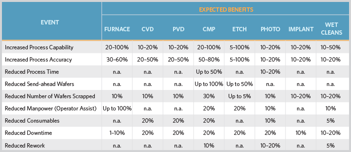
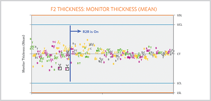
R2R control—In the early 1990s, model-based process control, known as R2R control in our industry, was first deployed on semiconductor manufacturing technologies such as chemical-mechanical planarization (CMP).[3] It was successfully demonstrated to improve process capability by improving control and reducing variability of qualities such as thickness and uniformity. Today R2R control is pervasive in most fabs and is a requirement in many front-end processes. Figure 1 illustrates the benefits that R2R control can provide, while table 1 summarizes the R2R control capabilities that are widely deployed in microelectronics front-end technologies today.[4] The microelectronics industry’s success with fab-wide model-based process control solutions positions us as a technology leader, and we continue to innovate in this arena, providing solution extensions such as non-threaded R2R control, and combining R2R control with capabilities such as S/D.[5,13]

alt-image

Figure 1: Example of R2R control success illustrating improvements in (1) closeness to target and (2) reduction in variability, both of which contribute to improvements in Cpk. (Source: Applied Materials)

alt-image

Table 1: Summary of typical applications of R2R control in microelectronics manufacturing and reported benefits. (Source: Applied Materials)

Real-Time S/D—While R2R control is arguably the most visible and talked about DT capability in the industry, real-time S/D modeling is another pervasive technology for microelectronics and a key component of the manufacturing DT family. Effective S/D solutions employ configurable control rules to model process and product flows in the fab, and determine what decisions should be made in scheduling across the fab and in dispatching at a particular tool. For example, understanding queue length, cycle times and transport times combined with product priorities (e.g., “hot lots”), can enable Applied RTD™ real-time S/D solutions to optimize WIP to a customer’s yield-throughput objective function using control rules. These rules can be easily updated to reconfigure the system in response to changing or unforeseen conditions such as changing demand or unscheduled downtime.[6] These and other innovations position the microelectronics industry to continue leading in this technology field, with Applied RTD real-time S/D solutions now being considered in other industry verticals that have stringent process control requirements, such as pharmaceutical and chemical.[7]

PdM and VM—While R2R control and S/D DT components are pervasive in fabs today, there are also emerging DT technologies that will become an integral part of fabs over the next few years. Primary among these are PdM and VM. Both of these technologies leverage the increased data consolidation, archiving, quality and analytics capabilities associated with the big data revolution to provide DT capabilities of equipment or component health and metrology processes, respectively. The keys to realizing the success of these emerging DT capabilities are:

  1. Understanding the complexities of implementing them in the highly dynamic and complex microelectronics manufacturing process environment;
  2. Providing a collaborative environment for integrating user, OEM and analytics solution provider knowledge into scalable and maintainable solutions; and
  3. Providing a methodology for secure data access so that solutions can be developed in a secure IP-protected environment.[8,9]

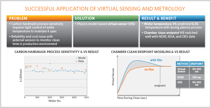
An example of this success in the VM arena is shown in figure 2. Here Applied Materials process- and equipment knowledge is combined with analytics to realize VM solutions for wafer temperature and chamber clean endpoint.[10] This same approach can be used to develop customized VM, virtual sensing and PdM solutions at customer sites that will become part of the factory integration solution over the next decade.

alt-image

Figure 2. Phenomenological (physics-based, statistically tuned) models will replace purely statistical models in virtual metrology/sensor solutions. (Source: “Virtual Sensors for APC in CVD,” APC Conference 2017)

THE NEXT STEP: COMBINING DIGITAL TWIN CAPABILITIES

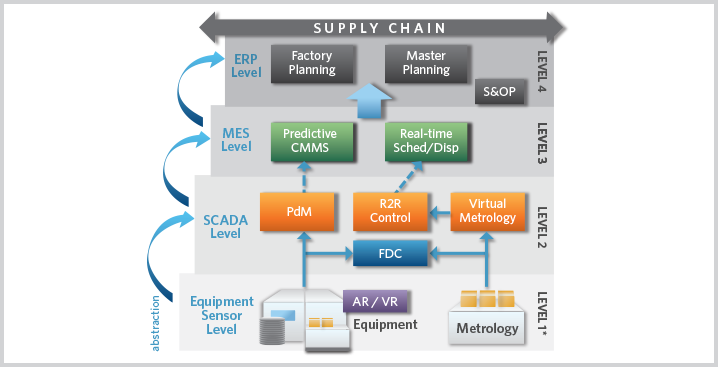
Existing and emerging DT capabilities all leverage the same data collection and management infrastructure and, as shown in figure 3, commonly interact with other DT and non-DT capabilities at a particular ISA1 level to provide targeted benefits.

alt-image

Figure 3. Illustration of DT capabilities at multiple levels leveraging the same data collection and management infrastructure. We can map DT capabilities onto the ISA-95 layered factory model and illustrate that (1) R2R control, VM and PdM are examples of process DTs at levels 1 and 2, and (2) rule-based systems for real-time S/D, as well as computer maintenance management systems (CMMS) that incorporate predictive components, are examples of process DTs at level 3.

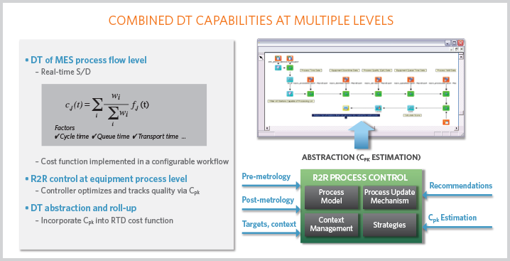
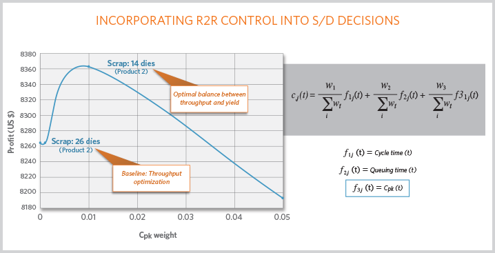
While these benefits are significant, a next generation of DT capabilities is now being realized, combining DT capabilities at multiple levels by abstracting the modeling information at one level, then using this information at a higher level to improve DT capability and precision. As an example, figure 4a illustrates how R2R-control DT capabilities at ISA-95 level 2 are abstracted to process capability (Cpk) predictions, which are then used by an Applied RTD system at level 3 to improve accuracy of S/D modeling and operation. Results (figure 4b) indicate that fab profit, computed as a function of yield and throughput of multiple products, can be improved if Applied RTD S/D decision-making is re-optimized to incorporate R2R Cpk prediction information. [13] At Applied Materials, engineers are engaging with customers to see if DT capabilities such as R2R control and RTD can be better integrated to further optimize decision-making.

alt-image

Figure 4a: Case study illustration of combining DT capabilities at multiple levels. On the lower right is a typical R2R control solution that leverages pre- and post-metrology along with dynamically updated process DT models to make recipe recommendations that improve process capability. It also has an ability to estimate Cpk over time. At the top of the figure is a typical Applied RTD DT implementation that uses a weighted sum of factors (such as cycle time and queue time, see equation) to determine where to route lots to achieve a throughput-quality optimization objective. In combining the R2R control and real-time S/D DT implementations, we incorporate the R2R Cpk estimation information as another factor in the Applied RTD optimization function. This allows for improved optimization as shown in Figure 4b.

alt-image

Figure 4b: Equipment process DT information incorporated into MES-level process flow.[13] Here we see the results of incorporating Cpk from a lower level R2R control DT into the Applied RTD DT optimization function. The capability of the Applied RTD S/D optimization is expressed as “profit” function, which is the Y axis. The plot illustrates that as we incorporate the Cpk factor into the optimization, the profit increases because expected quality is now incorporated into S/D decision-making. As we increase the weight of the Cpk factor, the expected profit increases to a maximum. If we raise the weight too high, the profit begins to decrease as quality-factor decisions begin to interfere with other optimization objectives such as throughput.

A VISION AND INDUSTRY ROADMAP FOR DT

While current and emerging DT capabilities provide significant opportunities in microelectronics manufacturing, it is important to understand the long-term DT vision so that we are poised to travel the road together. Fortunately the International Roadmap for Devices and Systems (IRDS) has taken on this task and defines the DT vision as “a state of fab operations where … real-time simulation of all fab operations occurs as an extension of an existing system with dynamic updating of simulation models.” [11] Many of the existing and emerging applications in the industry today will likely continue to evolve to more directly support this vision. Applications at all levels—from the equipment through the MES and ERP (as shown in figure 3)—will leverage big data capabilities, along with high levels of vertical and horizontal integration, to provide extensions into the virtual domain to support capabilities such as prediction, “what-if” analysis, and prescriptive operation.

ALREADY ON OUR WAY

As our industry moves forward to realize the IRDS DT vision, it is important to note that we are already having significant DT successes fab-wide at multiple levels, from the equipment through the MES. Our success in the DT space has resulted in part from focusing first on “what it does” (i.e., replicating a process) before we try to address “what it is” (i.e., replicating a physical asset such as a piece of equipment). Applied Materials has solutions that span the DT space and is committed to continued innovation, providing solution environments that allow us to bring together equipment, process and analytical knowledge to realize the DT vision.

For additional information, contact michael_d_armacost@amat.com.

Dr. James Moyne is an associate research scientist in the Mechanical Engineering Department at the University of Michigan, and a consultant to Applied Materials.

[1] The full SM vision, including an overview of SM tenets, was outlined in the December 2017 edition of Nanochip Fab Solutions. See “Moving Toward the Smart Factory,” Nanochip Fab Solutions, Applied Materials, Inc., Vol. 12/Issue 2/2017, December 2017

[2] Wikipedia: Digital Twin. Available online: https://en.wikipedia.org/wiki/Digital_twin

[3] Run-to-Run Control in Semiconductor Manufacturing, J. Moyne, E. Del Castillo, and A. Hurwitz, CRC Press, November 2000.

[4] Applied SmartFactory® R2R Control. Available online at: http://www.appliedmaterials.com/global-services/automationsoftware/e3-run-to-run-control-r2r

[5] Zou, J., et. al., “Minimizing pilot runs with non-threaded control technology,” Advanced Process Control Conference XXVI, September 2014. Available via: http://apcconference.com.

[6] Applied SmartFactory® Real-time Dispatching and Reporting. Available at: http://www.appliedmaterials.com/global-services/automation-software/apf-rtd-and-reporter

[7] S. Romero-Torres, J. Moyne and M. Kidambi, “Towards Pharma 4.0; Leveraging Lessons and Innovation from Silicon Valley,” American Pharmaceutical Review, February 2017. Available at: http://www.americanpharmaceuticalreview.com/Featured-Articles/333897-Towards-Pharma-4-0-Leveraging-Lessons-and-Innovation-from-Silicon-Valley.

[8] J. Moyne and J. Iskandar, “Big Data Analytics for Smart Manufacturing: Case Studies in Semiconductor Manufacturing,” Processes Journal, Vol. 5, No. 3, July 2017. Available at: http://www.mdpi.com/2227-9717/5/3/39/htm.

[9] J. Moyne, S. Mashiro, D. Gross, “Determining a Security Roadmap for the Microelectronics Industry,” Proceedings of the 28th Annual Advanced Semiconductor Manufacturing Conference (ASMC 2018), Saratoga Springs, New York, May 2018.

[10] Mungekar, H., et. al., “Virtual Sensors for APC in CVD,” APC Conference 2017, available via: http://apcconference.com.

[11] International Roadmap for Devices and Systems (IRDS), 2017 Edition: Factory Integration White Paper and Factory Integration Roadmap. Available at http://irds.ieee.org.

[12] ISA95, Enterprise-Control System Integration. Available at: https://www.isa.org/isa95/.

[13] Lopez, F., Moyne, J., Barton, K., and Tilbury, D., “Processcapability- aware scheduling/dispatching in wafer fabs,” Advanced Process Control Conference XXIX, October 2017. Available via: http://apcconference.com.