Products & Technologies

Products & Services
Company
Contact
Back to Menu
Products & Services
Products & Technologies
Services
Resources
Company
Contact
TABLE OF CONTENTS
A Letter from Ali Salehpour - Climb the Productivity Curve Faster
Leveraging the Digital Twin in Smart Microelectronics Manufacturing
STMicroelectronics Demonstrates Adaptive Endpoint Control System for 200mm CMP
Applied Materials Technology-Enabled Services Support Next-Generation Manufacturing
Maximize Output from Fleets of Tools
Industry 4.0 Reaches into the Subfab
The Last Word: Smart Transportation to Drive Semiconductor Content
Applied Materials Technology Enabled-Services Support Next-Generation Manufacturing
By David Lammers
As Moore’s Law has been stretched and the industry has become more global, more capital intensive, and more competitive, the focus of fab managers has expanded beyond device- and equipment breakthroughs to include significant advances in service technologies to boost the efficiency of semiconductor fabs.
The underappreciated reality is that the very trends grabbing so much attention— materials engineering, remote access, deep learning, and augmented reality—are radically changing how the Applied Global Services (AGS) group supports its forward thinking customers. From development through production, as device specifications become more stringent, technology-enabled services such as those from AGS can help customers achieve important yield, output and cost improvements at every step of the fab life cycle. These services are created on four pillars (figure 1):
- Surface technology, such as advanced cleaning and coatings solutions
- A large and growing network of experts who provide layers of specialized skills and experience for various solutions
- Digital tools such as advanced analytics and sensor modeling that empower field service engineers to more effectively resolve customer issues
- A tailored supply chain designed to address customers’ unique needs and streamline global operations to provide efficient, cost-effective solutions
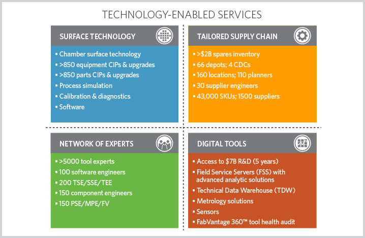
Figure 1. Applied technology-enabled services can help deliver significant improvements in yield, output and cost.

Jeremy Read is vice president of service marketing for AGS.
Semiconductor industry revenues exceeded $419 billion in 2017, and forecasts call for about $450 billion this year, up nearly 8%, according to market research firm Gartner. “This larger scale and rate of growth make it imperative that fabs operate at peak efficiencies,” said Jeremy Read, Applied Global Services (AGS) vice president of services marketing. “With nearly every fab operating now at full capacity, collaboration is essential.”
In such a fast-moving industry, semiconductor companies have begun to engage with AGS’s Services organization much earlier than ever before in the fab life cycle. Read said that by identifying and solving problems during the development and transfer-to-volume-manufacturing phases, customers can ramp volume production faster and reach optimum yields earlier, significantly improving revenues and margins (figure 2).
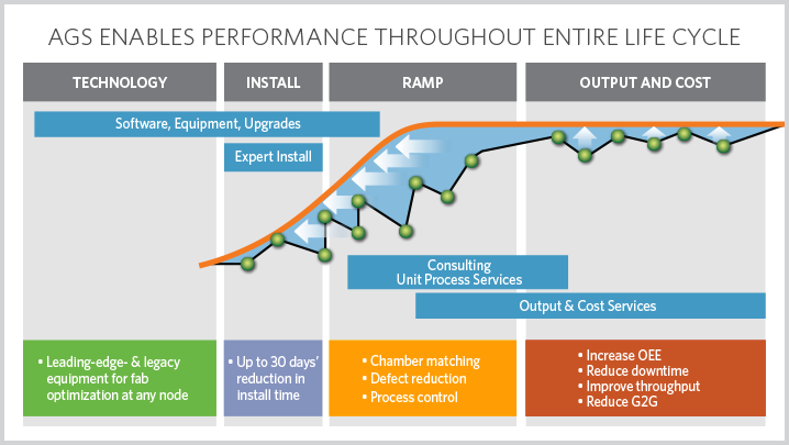
Figure 2. Identifying and solving problems before high-volume manufacturing can result in faster production ramp and earlier, higher yields.
“End-markets are more dynamic than ever, and manufacturers need to seize market share and generate return on invested capital as fast as possible,” Read said. “Quality output is always important, but today, speed and cost are huge competitive drivers. Customers’ support requirements are changing to reflect these new realities.”
SPEED IS A COMPETITIVE ADVANTAGE
Due to high capital costs and market competition, semiconductor manufacturers must ramp and yield more quickly than ever. During the startup phase, Applied’s installation teams, backed by software expertise, have sharply reduced the time needed to install and optimize tools. Applied has been able to achieve fab ramps 15% faster than traditional ramps, in terms of average cycle-time days. Further, the use of advanced analytics during startup has been shown to dramatically reduce troubleshooting time, improving overall cycle time by 25%.
Read said that technology-enabled services such as chamber matching and defect reduction from Applied’s FabVantage™ Consulting group allow customers to bring important new ICs to market on time.
In high-volume manufacturing, Applied helps maximize tool availability and reduce operating costs with faster troubleshooting, efficient preventive maintenance (PM) strategies, and extended-lifetime parts. In one case, AGS optimized PM procedures and schedules, helping a customer achieve a more than 4% uptime improvement for a fleet of ion implanters, and produce >150,000 additional wafers.
A LAYERED NETWORK OF EXPERTS
Applied customer engineers (CEs) are always on the front line of solving problems with customers’ production tools, and the company currently has over 5,000 of them deployed worldwide. Applied also has developed a comprehensive network of experts with specialized skills and training who augment the capabilities of a CE, often using digital tools and other supporting methodologies and expertise.
Brent Bloom, vice president of AGS central operations, said the company began refining the concept of a layered network of experts several years ago, with front-line CEs fortified by senior technical support engineers and a greatly expanded knowledge database. “We have been refining each level of expert to hone their specific area of proficiency. Every level and skill group has a certification process, including the dedicated tool install teams, tech support, software engineers, and others. In each case the training team has expanded the curriculum and certification programs,” Bloom said.
“Today each CE, regardless of background, has ready access to a network of experts. It is those layers of specialized expertise, backed by online tools, that has provided major opportunities to improve the customer experience. Sometimes we can detect issues in various operational behaviors even before the customer knows they are having a problem,” he said.
LEVERAGING BIG DATA
The amount of data generated daily by fabs is astounding (figure 3). So the challenge for fab managers is to tap into that data for information that will support faster time to yields.
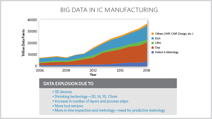
Figure 3. An explosion of data captured in fabs creates opportunities to improve production yields. (Source: VLSI Research and Applied Materials)
Applied Materials’ proprietary digital tools, algorithms, and models are tailored specifically to its tools and can transform raw data into actionable analytics to help reduce startup times, increase wafer output, reduce wafer scrap and improve yield— all while protecting customer data.
Analytics such as multivariate fault detection are proving capable of improving within-wafer performance. AGS’s multivariate chamber health index (CHI) monitors excursions in real time, and equipment health monitoring (EHM) tracks sensors that detail hardware activity.
In one case, a customer needed the ability to accurately predict thickness, dopant levels, and resistivity during process qualification of its epi chambers. AGS engineers developed analytical models to enable the customer to reduce process tuning time by 40%. In another instance, a CHI was developed that leveraged multiple critical sensors for the etching process so that a PM could be triggered before problems arose.
James Moyne, a consultant to Applied Materials and an associate research scientist in the Mechanical Engineering Department at the University of Michigan, said deep learning is one of many techniques that Applied can use to detect issues and boost yields. In the fabs, predictive metrology, predictive maintenance (PdM), and more data coming from more sensors on the tools, must all be coordinated into a knowledge gathering network. For relatively simple things, such as predicting how far in advance a single part needs to be replaced, PdM techniques have been proven to work, provided there is enough good data to develop adequate models.
Other problems involving more complex interactions remain harder to solve, but significant strides are being made in this area. Much of PdM’s success depends on how much data has been collected about previous failure patterns. “To understand all of the reactions leading up to a failure, we need enough accurate data. Without the right kinds of data, it is hard to have PdM systems. is like the golden child; just out of reach if you don’t have enough good data,” Moyne said. Predictive maintenance “has really strong potential ROI [return on investment]. It is where today’s fabs want to go.”
FABVANTAGE FOR CHALLENGING PROBLEMS
The FabVantage Consulting group helps customers address their most complex problems, whether they involve cost, efficiency or yield. For example, a FabVantage analysis for one customer resulted in reduced particle adders on a PVD TiN hardmask, from 16 to 9 particles per wafer. In another, FabVantage chamber-matching methodology matched critical dimensions (CD) and trench depth to achieve a chamber-to-chamber CD range of <0.5nm on a fleet of etch chambers in 2x-nm DRAM production (see related story in this issue on the new FabVantage capability for fleet optimization).
FabVantage consultants use advanced modeling and analytical tools and Applied’s extensive knowledge base to work with service teams to benchmark fab operations against best-in-class performance to ensure that tools are operating at optimum performance. Tools and recipes are audited, and sensor and on-wafer data is used to pinpoint key issues. This team is composed of experts with specialized, hands-on experience and tool knowledge. They leverage best known practices and specific expertise to help customers isolate problems and get to potential remedies faster.
TAILORED SUPPLY CHAIN
Applied maintains one of the industry’s largest global inventories of certified spare parts. With a robust logistics infrastructure, Applied offers multiple channels and spare part delivery programs to meet the unique needs of every fab.
Read summed it up: “Helping customers with human experts, knowledge databases, and a robust network of spares suppliers is part of our continual effort to serve a semiconductor industry striving to wring every ounce of productivity from its capital investments.”
For additional information, contact amitabh_sabharwahl@amat.com.