Products & Technologies
Back to Menu
Products & Technologies
Services
Resources
Table of Contents
A Letter from Ali Salehpour - Climb the Productivity Curve Faster
Leveraging the Digital Twin in Smart Microelectronics Manufacturing
STMicroelectronics Demonstrates Adaptive Endpoint Control System for 200mm CMP
Applied Materials Technology-Enabled Services Support Next-Generation Manufacturing
Maximize Output from Fleets of Tools
Industry 4.0 Reaches into the Subfab
The Last Word: Smart Transportation to Drive Semiconductor Content
150mm Alive and Kicking
By Mike Rosa, Ph.D.
Did you think chip making on 150mm wafers was a thing of the past? Think again. Many of the megatrends shaping our collective futures—mobility, autonomous driving and electric vehicles, 5G wireless communications, augmented- and virtual reality (AR/VR), and healthcare—depend on innovations created on the 150mm wafer size.
While attention is often riveted on the race to the leading-edge nodes, today important advancements in power devices, photodetectors and waveguides are being enabled by materials such as silicon carbide (SiC) and gallium arsenide (GaAs) wafers at 150mm, or even 100mm.
PHOTONICS DRIVE GaAs
GaAs has been used for decades in laser and LED technologies employed in applications such as photocopiers, DVD players and even laser pointers. In recent years, LEDs have propelled a further developmental push in compound semiconductor technologies. New advancements are coming from two classes of photonics applications: laser sources and waveguide technologies for data networks; and laser diode and photodetector technologies for advanced 3D imaging.
Devices fabricated on GaAs substrates have often been relegated to batch-toolstyle manufacturing due in part to the cost-sensitive nature of applications, notably LED lighting. Many of the traditional batch process steps involved the MOCVD growth of stacked material layers, with no intermittent lithography or etch processes until the very end of device fabrication when device contacts were created and singulation was performed.
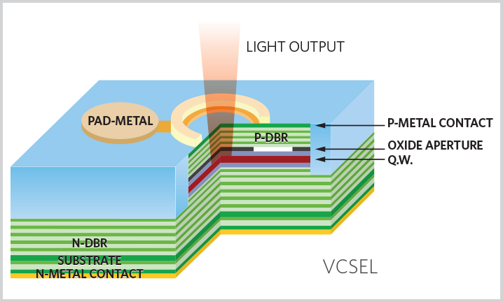
While much of that remains the same today, volume, yield and price pressures require some specific types of devices such as vertical cavity surface emitting lasers (VCSELs) to be manufactured using single-wafer processes where possible (figure 1). This is a departure from the traditional batch processing at a time when these III-V material technologies are finally working their way into broader consumer markets through applications like facial recognition.

Figure 1. Typical VCSEL device cross-section. An increasing number of these devices are manufactured in single-wafer processes vs. traditional batch processing.
iPHONE 150mm WAFER DEMAND STEADY
Apple’s iPhone X was the first consumer device to debut facial recognition in what could be considered an ultrahigh-volume consumer application. Up until this point (circa November 2017) GaAs substrate materials were used primarily in the RF front end (RFFE) of most cellular phones and other RF amplifier applications. In the iPhone X, 150mm GaAs substrate materials are used to fabricate RF components from the RFFE, along with VCSELs and photodetectors used in facial recognition.

Today, out of the roughly 121 die listed in the bill of materials (BoM) for the iPhone X, approximately 15 are made using 150mm wafers. This represents just over 12% of the total die count and approximately 2% of the total wafer area used to produce an iPhone X. The balance of the ICs in the iPhone X include roughly eighty-seven 200mm and nineteen 300mm die. By comparison, the silicon area for the 200mm and 300mm wafer sizes are approximately 32% and 66%, respectively.
The number of 150mm die and their corresponding area are both still relatively small compared to the larger 200mm and ever larger 300mm wafer sizes and the die applications they support. However, a review of prior iPhone BoMs reveals an interesting trend: the cumulative wafer area of devices made on 300mm has remained relatively flat since 2012 (a result of reduced node size offsetting the increased area demand required by increased complexity), while the wafer areas of devices made using 200mm and 150mm wafers have shown a CAGR of approximately 9.5% and 6%, respectively. That’s impressive growth underpinning the slowly expanding variety of More-than-Moore devices made at the 200mm and 150mm wafer nodes. Couple that with impressive Apple iPhone sales of more than $200M each year and you quickly begin to exceed 300,000 wafers at the 150mm node per year for the iPhone alone—and that is before considering other phone manufacturers or the proliferation of these power and photonic applications to other platforms.
SILICON CARBIDE APPLICATIONS ESCALATING
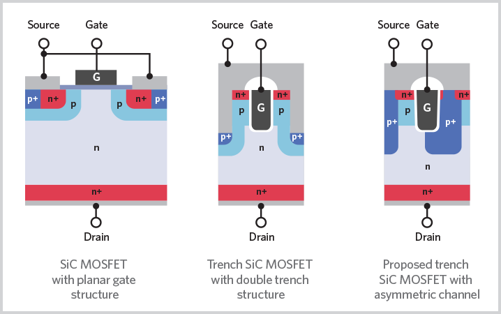
The second prominent area for 150mm wafer technologies is in the development of SiC power MOSFETs (figure 2). Today these devices are used mostly for high-power switching in industrial applications, but increasingly they’re also being used in the growing number of electric vehicles (EVs) that have begun to populate the highways. Today, there are two main types of SiC MOSFET structures in development or production: a planar MOSFET and a trenchgate MOSFET design.

Figure 2. SiC MOSFET device structures. (Source: Siemieniec, R., Infineon., EPE’17)
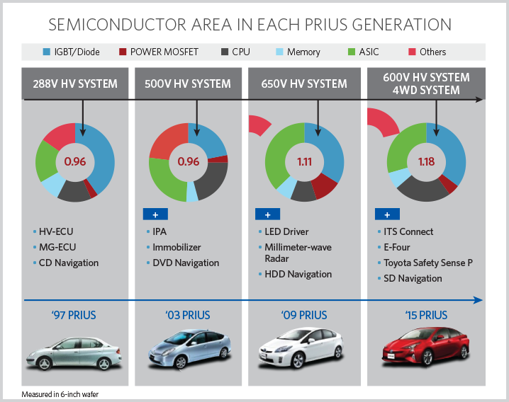
In 1997, the Toyota Prius consumed approximately 0.97 of a single 150mm wafer—shared among several applications, the largest of which was for power switching. By 2015, that number had risen to 1.18 wafers per vehicle (figure 3).

Figure 3. Evolution of 150mm wafer consumption in the Toyota Prius.
As the sophistication of power conversion systems around the car has increased, so too have the number of uses and performance requirements of the power modules. This is where SiC materials really excel. Compared with their silicon equivalents, the SiC power MOSFET can handle higher power and heat loads—an ideal trait for EVs that need to reduce overall weight to increase efficiencies. A consensus is emerging that the high breakdown voltage and high temperature operability of SiC MOSFETs ensures that SiC-based ICs will be key ingredients in future EVs.
How fast the EV market develops is an open question, however. At this point it should be noted that by some estimates EVs are forecast to represent approximately 5% of light passenger vehicles on US roads in the next decade.
With numbers like that and an increased number of applications for high-voltage switching around the vehicle, SiC wafer makers like Cree, Inc. (Durham, NC) have become increasingly bullish regarding the future of products made on 150mm wafers. Cree subsidiary Wolfspeed (Research Triangle, NC), a SiC power MOSFET device maker, is betting that the total available market (TAM) for SiC devices will swell to approximately $5B by 2023.

Cree divides the SiC device market into $2.5B for SiC power MOSFETs and $2.3B for SiC power inverters used in the photovoltaic market, with a remaining $200M in SiC devices used in consumer portable chargers. That is tremendous growth for a device industry still largely in its infancy and relegated to the 150mm wafer size.
In terms of raw wafer starts, Cree’s estimates are approaching 2M 150mm wafers by 2023, based on today’s current levels of 45K wafer starts, an impressive >110% CAGR through 2023. While Cree remains quite bullish on wafer starts and device TAMs, other sources such as market research firm Yole Développement are taking a more conservative view, predicting around 150K wafer starts by 2023, with a CAGR of just over 50% through 2023, based on today’s levels.
TOOL REQUIREMENTS FOR 150mm MANUFACTURING
What does all this mean in terms of tool requirements? While much of the magic in SiC remains in the growing of the wafer crystal ingot itself, to produce the SiC wafer there are unique additional post-ingot steps such as grinding, CMP, SiC epi, implant, inspection, CVD and PVD. SiC wafers pose many challenges due to their semitransparent nature and material hardness, which require equipment redesign or modification for key process steps, including CMP, SiC epi (>1600°C), implant (>500°C) and inspection of crystallographic defects specific to SiC growth.
THE FUTURE LOOKS BRIGHT
Applied Materials continues to invest in the R&D of production equipment required for current and future devices made on 150mm wafers. We are also keeping a close eye on demand for devices made on advanced materials, including photonics and SiC power MOSFETs.
While R&D toward 200mm wafer materials continues for both classes of device mentioned here—power and photonics—it is clear that the future for 150mm wafer technologies is a bright one. Indeed, 150mm manufacturing looks to be very much alive and kicking.
For additional information, contact mike_rosa@amat.com.
