Producer® Selectra® Etch
The Producer Selectra Etch system introduces unprecedented capabilities for sustaining the momentum of Moore’s Law through further scaling of 3D logic and memory chips. This process can remove target materials with unprecedented selectivity to one or more films.
Features in chip designs are becoming progressively smaller with higher aspect ratios and are being packed more densely in advanced integrated circuits. The precision with which devices are patterned or cleaned is crucial for their ultimate reliability and performance. Incomplete removal of a material or enlargement of critical dimensions caused by inadequate selectivity can have detrimental consequences to device performance and yield. Pattern deformation of high aspect ratio features (line bending and pattern collapse) can also impact yield of next-generation devices.
The Selectra system addresses each of these concerns. Its unique process makes possible atomic-level etch control for advanced FinFET, uniform recess for 3D NAND, and damage-free clean for high aspect ratio DRAM structures.
The system employs a radical-based chemistry to deliver tunable selectivity for removal of a variety of dielectric, metal, and semiconductor films with atomic-level precision. This technology is pivotal for advancing Moore’s law by extending the boundaries for today’s FinFET devices, and enabling gate-all-around structures of tomorrow.
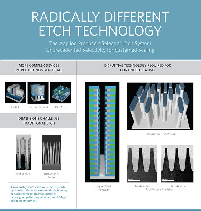
Insufficient selectivity of traditional processes causes greater recessing of tungsten near the top of the NAND stack than at the bottom, resulting in degraded device performance.

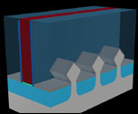
Lack of material selectivity leads to wet etch chemistry widening all layers in a cylindrical DRAM capacitor, producing an undesirable increase in the diameter.
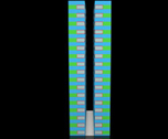
Crystal-plane-dependent wet etch process results in polysilicon residue remaining in small spaces in advanced logic transistors
Capillary forces ("stiction") during the drying step that follows wet etch causes collapse of high aspect ratio features.
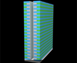
The tungsten selectivity of the Selectra process can be tuned to produce a highly uniform recess etch throughout the entire 3D NAND stack.
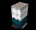
The Selectra process can be tuned to act selectively only on those layers where the cylinder’s diameter must be widened.
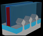
The Selectra process removes all traces of polysilicon residue, leaving gate oxide
features clean and ready for metal gate deposition.
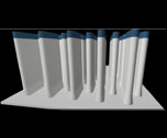
The completely dry Selectra process preserves the structural integrity of fragile features.

