Back to Menu
업계를 근본적으로 변화시키기 위한
시스템 관점의 접근 방식
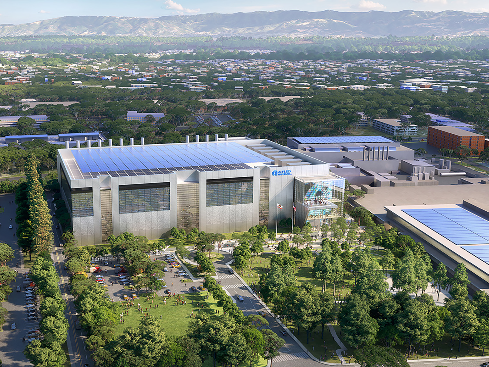
당사는 실리콘밸리에 세계 최대 규모의 최첨단 반도체 공정 기술 및 제조 장비 협업 시설인 EPIC 센터™를 설립하고, 인도 벵갈루루에 협업 엔지니어링 센터를 설립하여 혁신의 방식을 근본적으로 변화시킬 계획입니다.
당사는 목적 지향형 제품을 만들고 기존 제품의 환경 성능을 향상시키는 등 혁신 방식을 혁신하여 팹의 에너지, 화학적, 물리적 사용량을 크게 줄이기 위해 고객과 협력하고 있습니다.
어플라이드 머티어리얼즈는 친환경 제품 포트폴리오, 업그레이드 및 어플라이드 머티어리얼즈 서비스 계약을 통해 고객이 자본 투자 가치를 극대화하고 탄소 배출량을 줄일 수 있도록 지원하고 있습니다.
공급망 파트너와 협력하여 전략적인 10년 로드맵인 SuCCESS2030을 통해 비즈니스 가치와 표준에 부합하는 보다 지속 가능한 공급망을 구축하기 위한 노력을 이어가고 있습니다.
지속가능성 시스템 전문가 조직
지속가능성 시스템 전문가 조직은 엔지니어링 설계 팀이 보다 지속 가능한 제품과 프로세스를 개발할 수 있도록 지원합니다. 그 결과는 팹 및 서브팹을 위한 목적 지향형 제품 및 서비스의 확장된 포트폴리오에서 확인할 수 있습니다.
SuCCESS2030
환경 및 사회적 지속가능성을 위한 공급망 인증(SuCESS2030)은 비즈니스를 지원하기 위한 ESG 공급망 전략을 강화하기 위한 10년 로드맵입니다. 2040년까지 넷제로를 달성하기 위해 공급업체와 협력하여 온실가스 배출량 감축 계획을 수립하고 재생 에너지 조달을 지원하는 등 다양한 노력을 기울이고 있습니다.

책임있는 광물 조달(Responsible Mineral Sourcing)
어플라이드 머티어리얼즈는 제품에 사용되는 광물재료를 책임감 있게 조달하기 위해 최선을 다하고 있습니다. 당사는 책임있는 광물 조달 및 공급망 관리를 위한 연합체인 책임 광물 이니셔티브의 회원사이며, 공급업체가 책임 광물 인증 프로세스(RMAP) 표준을 준수하는지 검증하는 데 노력하고 있습니다.

PFAS에 대한 성명서
당사는 공정 화학물질에 대한 PFAS 책임 접근법의 일환으로 기술적으로나 상업적으로 가능한 경우 과불화화합물(PFAS)을 우선적으로 제거하고, 필요한 경우 비 PFAS 대체물 개발에 주력하고 있습니다.
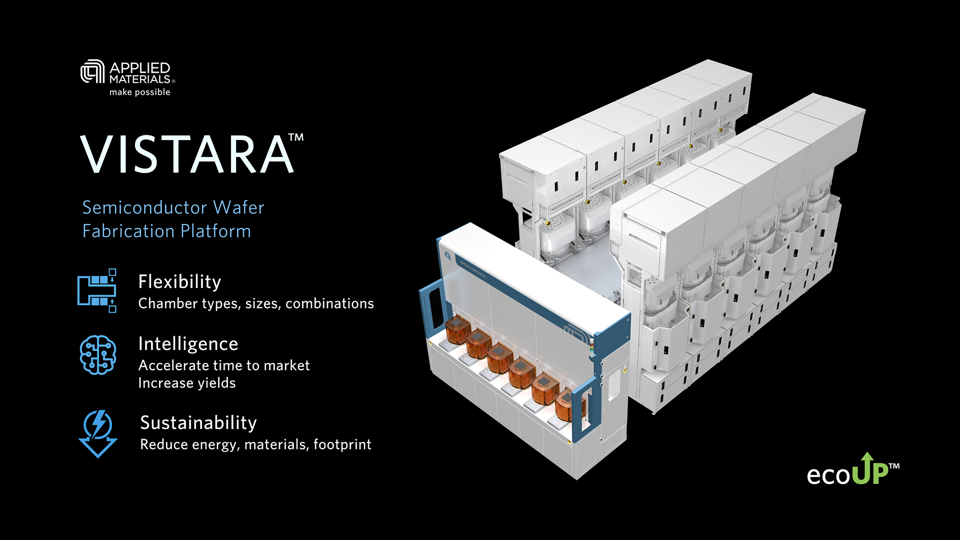
Vistara™
Vistara는 더 많은 유형과 크기의 챔버를 사용하는 통합 재료 솔루션 레시피를 지원하도록 설계된 최초의 특수 제작 플랫폼입니다. 단일 툴 내에서 여러 공정 단계를 결합하고 최적화하여 플랫폼 에너지 소비를 약 35% 절감하고 식각 애플리케이션의 화학물질 사용량을 약 30% 줄입니다.


Centura™ Sculpta™ 패턴 쉐이핑 도구
Sculpta는 웨이퍼 공정 과정에서 EUV 마스크 레이어 전공정을 제거하는 업계 최초의 패터닝 기술을 특징으로 합니다. Sculpta는 상당한 자본 및 제조 비용 절감 외에도 웨이퍼당 15kWh 이상의 에너지 절감, 웨이퍼당 이산화탄소 0.34kg 이상에 해당하는 온실 가스 배출량 감소, 웨이퍼당 약 15리터의 물 절약이 가능합니다.

iSystem™ 컨트롤러
고객사인 TSMC와 공동으로 개발한 iSystem 컨트롤러는 반도체 제조 장비의 작동에서 전력 사용량 측정을 자동화하여 표준공정에 대한 실제 에너지 사용량을 측정합니다. iSystem 컨트롤러는 고객이 에너지 관련 비용을 약 20% 절감할 수 있도록 도와줍니다.

에코트윈™
에코트윈은 레시피와 작업을 모니터링하고 모델링하여 칩 제조업체가 팹에서 에너지 최적화를 추진할 수 있도록 지원하는 디지털 트윈입니다. 에코트윈 소프트웨어 도구는 팹과 서브팹 모두에서 탄소 배출량 및 관련 소비 매개변수에 대한 상세 보고서를 자동으로 생성하여 고객이 소비를 줄일 수 있는 기회를 찾을 수 있도록 지원합니다.
3x30 목표
2030 목표 |
혁신* |
|---|---|
|
반도체 제품의 웨이퍼당 에너지 사용량을 2030년까지 2019년 대비 30% 절감 |
웨이퍼당 평균 에너지 사용량은 판매 제품 구성의 변화로 인해 계속 감소했습니다. 기존 제품과 출시 제품에 새로운 에너지 절감 개발을 통합하면서 3x30 목표를 달성 또는 초과 달성할 수 있는 궤도에 올랐습니다. |
|
2030년까지 반도체 제품의 웨이퍼당 화학물질 소비로 인한 영향 2019년 대비 30% 감축 |
제품 사업 부서의 지속 가능성 시스템 전문가 조직과 엔지니어링 파트너는 공정 화학, 대체 공정 화학 및 개선된 저감 솔루션에 대한 수요 감소를 통해 화학적 영향을 크게 줄일 수 있는 여러 제품의 개발을 지속적으로 추진하고 있습니다. 이러한 이니셔티브 중 일부는 수년에 걸쳐 노력해야 할 것으로 예상되지만, 당사는 3x30 목표를 달성 또는 초과 달성할 수 있는 궤도에 올랐습니다. |
|
반도체 제품 생산단위 비율당 툴이 차지하는 면적 2019년 대비 30% 감축(sqm/wph) |
현재까지의 툴이 차지하는 면적감소는 대부분 기존 툴 아키텍처의 생산성 향상의 결과입니다. Vistara와 같은 신제품 아키텍처가 고객에게 대량 출하를 시작함에 따라 툴이 차지하는 면적은 더욱 감소할 수 있으며 3x30 목표를 달성하거나 초과할 것으로 예상됩니다. |
SuCCESS2030 목표
2030 목표 |
혁신* |
|---|---|
|
감축 목표에 대한 상위 공급업체 및 파트너의 온실가스 데이터 수집 |
2023 회계연도 80여 개 협력업체 대상 온실가스 조사 실시 |
|
RBA Code of Conduct 및 어플라이드 머티어리얼즈 Standards of Business Conduct (SBC) 준수 추진 |
2023년 50개 이상 상위 협력업체 대상 감사 실시 |
|
2024년까지 여성 및 소수자 소유 기업 관련 지출 비율 및 대표성을 높여 2027년까지 다양성 지출 10억 달러 달성을 목표 |
다양성 지출을 전체 글로벌 공급업체 지출의 3.8%로 늘리고, 2023년에는 인증된 다양한 공급업체와 5억 9400만 달러를 지출한다는 중간 목표 달성 |
|
2023년 말까지 공급망의 80%를 재활용 가능한 콘텐츠 포장으로 전환 목표 |
2023년까지 어플라이드 포장재의 약 80%가 재활용 가능한 소재로 제작 |
*별도 언급 시까지 2023 회계연도까지 누적 기준
