Products & Technologies
Back to Menu
Products & Technologies
Services
Resources
Taking a system-view approach
to fundamentally transform our industry.
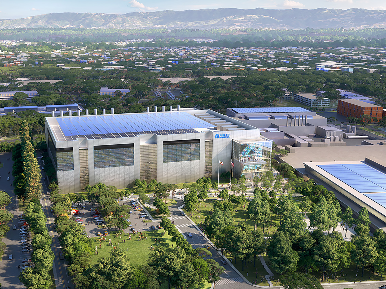
We’re building the world’s largest and most advanced facility for collaborative semiconductor process technology and manufacturing equipment R&D in Silicon Valley, the EPIC Center™, and planning a collaborative engineering center in Bangalore, India, to fundamentally transform how innovation happens.
We’re working alongside our customers to innovate the way we innovate—creating purpose-driven products and advancing the environmental performance of existing products—to significantly reduce the energy, chemical and physical footprints of fabs.
Applied is enabling customers to maximize the value of their capital investment and lower emissions through our growing portfolio of eco-advantaged products, upgrades and Applied Material service agreements.
In collaboration with our supply chain partners, our strategic 10-year roadmap, SuCCESS2030, guides our progress toward creating a more sustainable supply chain aligned with our business values and standards.


Sustainability Systems Center of Excellence
Sustainability Systems Center of Excellence supports our engineering design teams in developing more sustainable products and processes. The results can be seen in our expanding portfolio of purpose-driven products and services for fab and subfab.

SuCCESS2030
Supply Chain Certification for Environmental and Social Sustainability (SuCESS2030) is our 10-year roadmap for strengthening our ESG supply chain strategy to support our business. We are working with our suppliers on creating a path to reach net zero by 2040, including establishing a GHG emissions reduction plan and assisting them in procuring renewable energy.

Responsible Mineral Sourcing
Applied Materials is committed to the responsible sourcing of minerals used in our products. We are a member of the Responsible Minerals Initiative, and we work to validate that our suppliers conform with Responsible Minerals Assurance Process (RMAP) standards.

Statement on PFAS
We are prioritizing the elimination of per- and polyfluoroalkyl substances (PFAS) where technically and commercially feasible, and the development of non-PFAS alternatives where needed, as part of our “PFAS Responsible” approach to process chemicals.

Vistara™
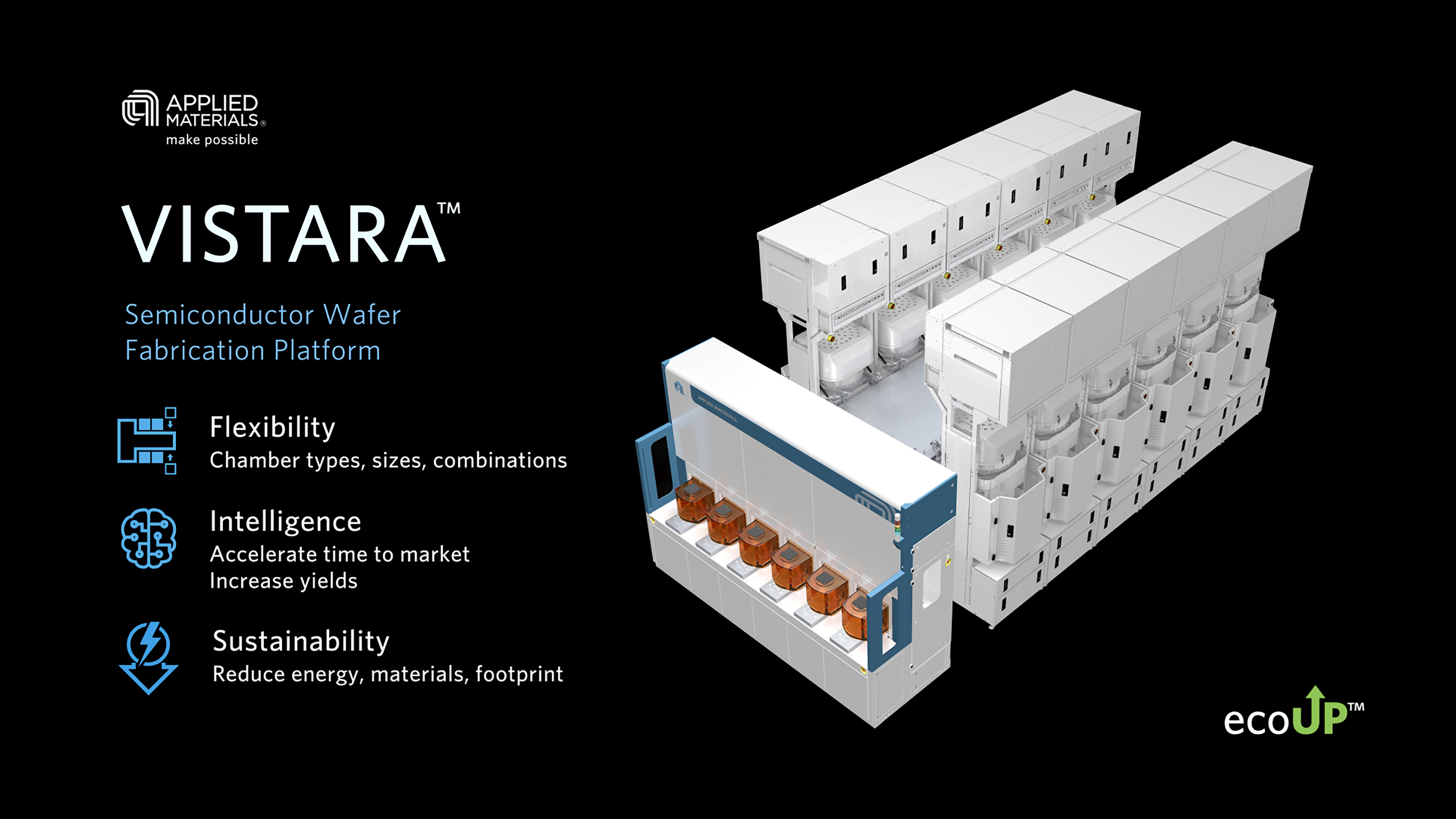
Vistara is our first purpose-built platform, designed to support Integrated Materials Solution recipes using more types and sizes of chambers. It combines and co-optimizes multiple process steps within a single tool, resulting in an estimated 35% reduction in platform energy consumption and about 30% reduction in chemical footprint for etch applications.


Centura™ Sculpta™ Pattern-Shaping System
The Sculpta features industry-first patterning technology that eliminates an entire EUV mask layer from a wafer process flow. In addition to significant capital and manufacturing cost savings, Sculpta enables energy savings of more than 15 kWh per wafer, direct GHG emissions reduction of more than 0.34 kg of CO2 equivalent per wafer and water savings of about 15 liters per wafer.


iSystem™ Controller
Developed in collaboration with our customer TSMC, the iSystem Controller automates measurement of power usage from the operation of semiconductor fabrication tools, gauging actual energy use against a baseline. The iSystem controller can help customers reduce energy-related costs by about 20%.


EcoTwin™
EcoTwin is a digital twin that can monitor and model recipes and operations so chipmakers can drive energy optimization in their fabs. The EcoTwin software tool automatically generates detailed reports of carbon footprint and related consumption parameters from both the fab and subfab to help customers identify opportunities to reduce consumption.

3x30 Goals
2030 Goal |
Progress* |
|---|---|
|
Reduce equivalent energy consumption per-wafer pass for semiconductor products by 30% by 2030 from 2019 baseline |
Average per-wafer energy use continued to decrease due to changes in the mix of products sold. As we incorporate new energy savings developments into our existing and upcoming products, we are on track to meet or exceed our 3x30 target. |
|
Reduce the impact from chemical consumption per-wafer pass for semiconductor products by 30% by 2030 from 2019 baseline |
Sustainaibility Systems Center of Excellence team and its engineering partners in the product business units continue to pursue development of multiple products that can significantly reduce chemical impact through reduced demand for process chemicals, alternative process chemistries and improved abatement solutions. Some of these initiatives are expected to be multi-year efforts, but we are on track to meet or exceed the 3x30 target. |
|
30% reduction in tool footprint per production unit ratio (sqm/wph) for semiconductor products from 2019 baseline |
Footprint reduction to date is largely the result of productivity improvements in existing tool architectures. As new product architectures, such as Vistara, begin volume shipments to customers, footprints can be further reduced and are expected to meet or exceed the 3x30 target. |
SuCCESS2030 Goals
2030 Goal |
Progress* |
|---|---|
|
Collect GHG data from top suppliers and partner on reduction targets |
Conducted GHG surveys with over 80 suppliers in fiscal 2023 |
|
Drive compliance with RBA Code of Conduct and Applied Materials Standards of Business Conduct (SBC) |
Conducted audits of over 50 top-tier suppliers in 2023 |
|
Increase the percentage of spend with, and representation of, women- and minority-owned businesses by 2024, aiming to reach $1 billion in diverse spend by 2027 |
Met our interim goal of increasing diverse spend to 3.8% of total global supplier spend, spending $594 million with certified diverse suppliers in 2023 |
|
Transition the supply chain to recyclable content packaging, with a target of 80% by year-end 2023 |
Through 2023, an estimated 80% of Applied packaging materials were made from recyclable materials |
*Cumulative through fiscal 2023 unless otherwise noted

