
STMicroelectronics Demonstrates Adaptive Endpoint Control System for 200mm CMP
By Leonardo Caudo, STMicroelectronics and Cosimo Patini, Applied Materials
Yield enhancement has always been a key goal for semiconductor manufacturers, but has taken on increased urgency given the strong demand for chips to meet a diverse and growing set of applications.
However, the stringent device-performance and reliability requirements and process-control rules imposed by some of these applications, such as automotive, make achieving higher yields difficult.
This is especially true for die at the edge of the wafer. Wafer edge-to-center film non-uniformity (also known as within-wafer non-uniformity or WIWNU) negatively impacts the final electrical performance of these devices, reducing their yield.
To decrease WIWNU, STMicroelectronics and Applied Materials are collaborating on the qualification of an improved process control solution that Applied has developed to fabricate 130nm bipolar-CMOS-DMOS (BCD) technology for automotive applications.
This solution is the industry’s first real-time, closed-loop Adaptive Endpoint control system for a 200mm chemical-mechanical planarization/polishing (CMP) platform, implemented on an Applied Materials 200mm Mirra™ CMP tool. Although 300mm CMP tools already have this kind of control system, it has so far been lacking on 200mm platforms.
Now undergoing pre-production testing with various CMP oxide/poly processes, the 200mm Adaptive Endpoint control system has demonstrated the ability to compensate for process drift caused by incoming film variability and aging of consumables.
This capability can increase device yields at the wafer edge. To date, the new control system has shown a WIWNU range improvement of up to 40%.
AN INFLECTION POINT FOR 200mm CMP
STMicroelectronics invented and is a leader in BCD technology, which integrates analog, digital and power technologies to address a broad range of power management, data acquisition and actuator applications for automotive and other uses. The STMicroelectronics R2 fab in Agrate Brianza near Milan, Italy, is their R&D center for BCD technology, where advanced processes and devices are developed on an ongoing basis.
In late 2016, STMicroelectronics began working with Applied Materials on a project encompassing a series of hardware and software upgrades and improvements to a 200mm Mirra tool at the R2 fab. This work included implementing the Adaptive Endpoint control system and retrofitting with Applied’s powerful Vita™ controller to replace the tool’s original VME-based single-board controller.
The Mirra tool with Adaptive Endpoint control system was brought online for initial testing in 2017, and is currently in pre-production for inter-metal dielectric (IMD) and pre-metal dielectric (PMD), and in development for polysilicon deep trench isolation (DTI). Volume production of 130nm BCD devices is expected to begin later in 2018.
Planarization in a tight within-wafer thickness range is demanding with BCD’s three integrated technologies because all CMP steps—shallow trench isolation (STI), DTI, PMD and interlayer metal dielectric (IMD)—are involved. The challenge is more difficult because depth-of-focus (DOF), defects (nitride or polysilicon residue) and contact chain resistance must also meet specifications at the same time.
A TIGHT COUPLING
In the past, advances in CMP were driven by developments such as the introduction of highly selective slurries, new generations of polishing pads, and new types of conditioner disks with better wafer-edge removal rate performance.
Now, the next step forward will be achieved by linking the aging of CMP consumables directly to the process control system in a closed-loop configuration so that polishing-head pressure zones can be adjusted to wafer conditions in real time.
Applied Materials already offers a 200mm Titan Contour™ wafer-carrier head featuring six independently controlled pressure zones to compensate for WIWNU. Applied also offers 200mm FullScan™ endpoint technology (figure 1) that can collect interferometric or reflectivity endpoint traces across different areas of a wafer.
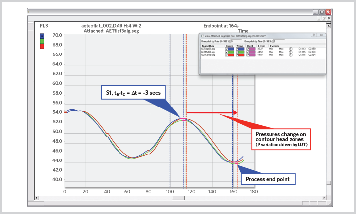
Figure 1. Applied Materials FullScan™ endpoint technology can report the interferometric layer signal from the edge and center of a wafer during polishing to determine the change in endpoint time.
However, until now, both have worked independently of each other in an open loop. This means that any incoming film variability, or any side effects from aging CMP consumables, cannot be taken into account. The result is a large WIWNU range following CMP, which can impact device performance and ultimately yields.
The new Adaptive Endpoint control system couples the operation of Applied’s Titan Contour head with the change in endpoint time (the “delta time”) collected by the FullScan endpoint interferometric curve. This is done via a lookup table and enables pressure zones in the Titan Contour head to be adjusted in real time based on actual on-wafer data to reduce WIWNU (figures 2 and 3).
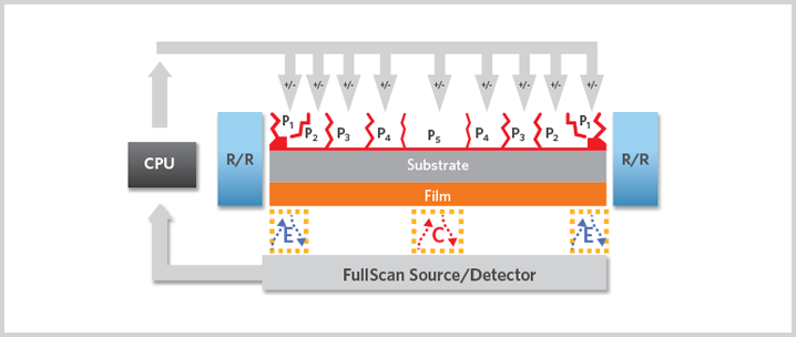
Figure 2. Adaptive Endpoint control system topology.
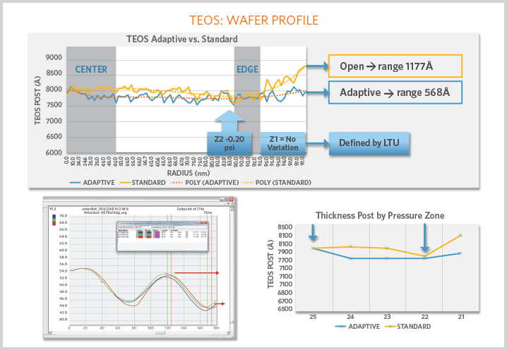
Figure 3. Post-CMP range improved by Adaptive Endpoint application.
The idea is that a within-wafer thickness range during CMP polishing generates an interferometric trace phase-shift range. A longer time indicates slower CMP polishing, while a shorter time means CMP processing is going faster. The delta time between these FullScan segment traces can be used to tune the pressure zones in the Titan Contour head to fine-tune the CMP process as needed to bring WIWNU within the desired range.
In order to increase the definition and repeatability of the traces, STMicroelectronics and Applied Materials have also taken steps to minimize the interferometric noise at the wafer edge.
CONCLUSION
The in-situ, within-wafer, real-time process control of the new Adaptive Endpoint system significantly enhances final CMP process performance. It also creates the opportunity to capture incoming variability (i.e., variations in incoming film uniformity) and process performance drift arising from aging consumables. In turn, these capabilities can lead to improved overall equipment efficiency.
For additional information, contact cosimo_patini@amat.com.

Mr. Caudo is Dielectric and Polysilicon CMP Team Leader at STMicroelectronics
Mr. Caudo is Dielectric and Polysilicon CMP Team Leader at STMicroelectronics

Mr. Patini is Technology Project Manager at Applied Materials
Mr. Patini is Technology Project Manager at Applied Materials