
New Generation 10+ Fabs Enable Bigger, Brighter, Better TV Displays
APPLIED MATERIALS ENABLES 65-INCH, 8K-RESOLUTION, G10+ OLED TVS
By Kerry Cunningham
Consumers are moving to larger and larger televisions, attracted by the chance to have a more immersive experience and the ability to see what is on the screen from farther away. TV sizes continue to grow by 1 to 1.5 inches per year, and sales of TVs with 65” or larger screens—so-called Gen10+ flat panel displays (FPDs)—are growing exponentially (figure 1).
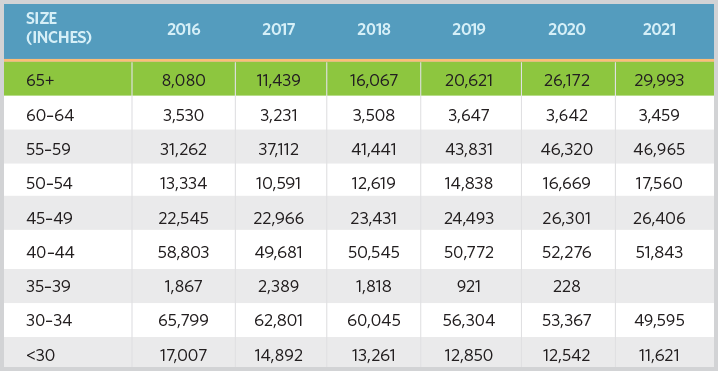
Figure 1. Television shipments by screen size, in thousands of units. The green row shows that shipments of 65+” TVs grew from about 8 million in 2016 to 11.5 million last year, and are expected to reach some 30 million in 2021. (Source: IHS)
Display manufacturers are quickly ramping new fab capacity to meet the demand. Figure 2 compares fab capacity additions for all sizes of FPDs from 2013–2019(e), indicating that larger sizes strongly dominate manufacturers’ production plans.
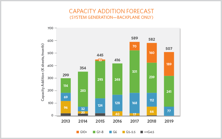
Figure 2. FPD manufacturers are adding significant production capacity for Gen10+ FPDs, which are represented by the orange bar segments. Each bar shows the total production capacity added each year (2018–19 estimated), in thousands of sheets per month. (Source: Applied Materials)
This growth is being driven by the emerging 8K ultrahigh-definition (UHD) resolution of the screens, organic LED (OLED) technology, and forthcoming 5G broadcasting formats.
- 8K: The more pixels on a screen, the higher the image quality. The 8K specification calls for 7680 horizontal pixels x 4320 vertical pixels. By comparison, full HD is 1920 x 1080 pixels, meaning that 8K has 16 times as many. At present, 4K is becoming mainstream and services like Amazon Prime Video, Netflix, YouTube, 4K Blu-ray, BT and Sky are now producing content in 4K. For the first time in its history, the 2018 FIFA World Cup was broadcast in 4K. Content broadcast in 8K is expected to appear in time for the 2020 Summer Olympics in Tokyo.
- OLED TV: OLED TVs are compelling because they are lightweight and thin, require no backlight, and produce vivid color and true-black contrast ratios. OLED adoption in the premium segment of the market is growing (figure 3), with TV manufacturers adding features such as “Crystal Sound” to further differentiate OLED from LCD TV.
- 5G: The current methods for TV service delivery are cable, satellite, Internet protocol TV (IPTV) and ground broadcast service. The term 5G TV refers to the ability to watch standard TV broadcasts over a 5G mobile network connection rather than via fixed broadband, cable, or satellite. This 5G service will be able to support a 1 Gbps data-throughput rate, which is fast enough to support broadcast television. It will also provide the ability to beam TV content to mobile devices without the need for a fixed Internet connection. A combination of low latency, speed and mobility will also enable more immersive virtual reality (VR) video content. It’s expected that 5G will appear commercially around 2020.
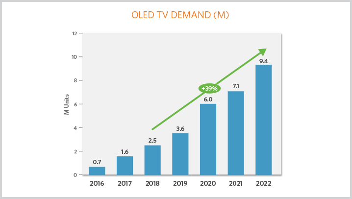
Figure 3. The graph shows that OLED TV shipments (in millions of units) doubled from 2015 to 2016, and doubled again from 2016 to 2017. Continued strong growth is anticipated for the next several years. (Source: IHS, Applied Materials)
The market for large, high-end TVs is the most profitable one for television makers, and it sets the trends for next-generation TV technology as well. But given that consumers expect low costs, the economic mass production of Gen10+ televisions comes with some critical requirements. The main ones are larger glass substrates, tighter process specifications, and the use of metal oxide thin-film transistors (TFTs) in the FPD backplane.
LARGER SUBSTRATE GLASS FOR GEN 10+ TVS
A key to achieving high margins in the high-end TV segment is the ability to fabricate these TV screens on very large sheets of glass substrate. This leads to production efficiencies because more TV screens can be produced per substrate, maximizing revenue per area of glass.
For 65” or larger TVs, glass substrates larger than those currently used for Gen 8.5 are essential. The Gen10+ substrate size is 2840mm x 3370mm, 180% larger than Gen 8.5 (figure 4).
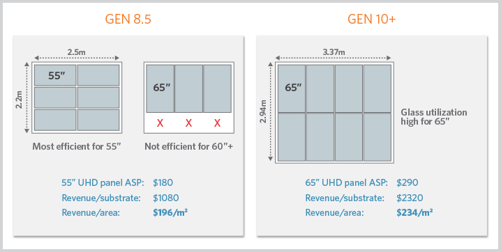
Figure 4. Revenue per area of glass for Gen 8.5 and Gen10+ substrates ($196/m2 vs. $234/m2, respectively). With Gen10+ production more TV screens can be produced per substrate, maximizing revenue per area of glass.
HIGHER RESOLUTION DEMANDS SMALLER PIXELS, TIGHTER PROCESS SPECS
Achieving higher resolution in FPDs of this size is challenging. As pixel sizes shrink, there must be a 3X improvement in process uniformity with a 10X density reduction in particles versus Gen 8.5 in order to maintain factory yield expectations of ~90%. As the portion of substrate glass devoted to one TV screen becomes larger, just one “killer defect” can render a large section of that expensive substrate useless (figure 5).
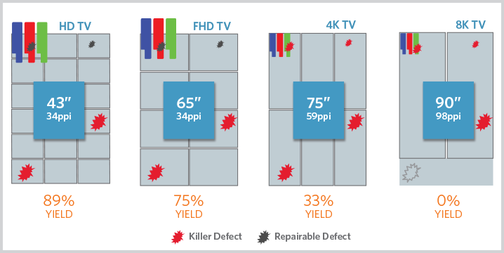
Figure 5. Tighter process control and significant particle reductions are essential for 8K resolution as the size of TV screens increases.
Also, because an 8K Gen10+ TV screen has more than 33 million pixels, reducing the amount of power needed to drive pixel brightness at this resolution is paramount. In each unit cell, the TFTs, storage capacitor electrodes, signal bus lines and black matrix material constitute opaque areas. The open area through which light can pass is called the aperture. Accordingly, an important design consideration is to maximize the aperture ratio, letting as much light as possible pass through each unit cell so that less power has to be dedicated to display brightness.
Doing this requires much tighter process specifications than with previous generations of TV screens (figure 6).
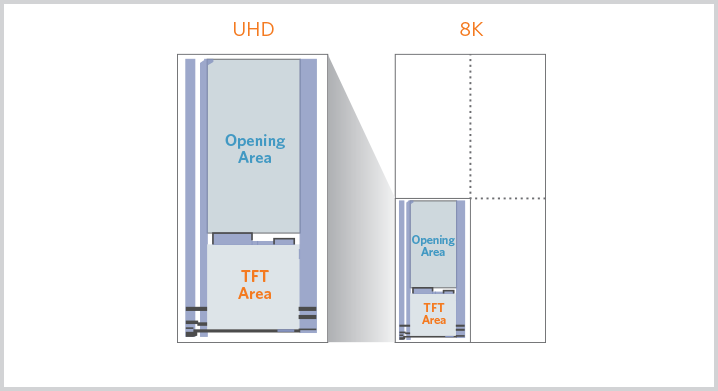
Figure 6. At 8K resolution, it is critical to increase the pixel aperture ratio, or the size of the aperture (open area through which light can pass) versus pixel TFT area. The figure shows the requirement schematically.
METAL OXIDE ELECTRODES
The use of backplanes with TFTs made from a metal oxide (MOx) material known as IGZO is emerging as the most effective solution for large-area 8K OLED TVs in terms of cost and performance.
IGZO-based TFTs offer high electron mobility, facilitating higher aperture ratios, low leakage currents, a high on/off ratio for low device power consumption, and deviceperformance stability. They are also compatible with current-driven OLEDs and 3D displays, provide image uniformity over large areas, are transparent, and have long lifetimes.
A major challenge, though, is that the IGZO material keeps interacting with its surroundings during device fabrication. Its structure can change as a result, affecting its performance. That means great care must be taken during the process steps required for device fabrication and integration: CVD, PVD, dry etch and annealing (figure 7).
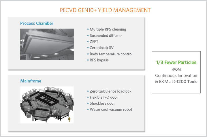
Figure 7. Tight process control is essential to achieve high yields of stable, uniform MOx TFT devices. Shown are some of the variables that must be considered during PECVD of Gen10+ FPDs.
The key to producing uniform and stable TFT devices is to tightly control the IGZO oxygen levels/oxygen vacancies and hydrogen levels during each fabrication step. Tight control leads to improved gate insulation, while high-quality SiOx reduces interface trapping, minimizes hydrogen content, and boosts etch-stop (ES) layer performance to protect the IGZO layer during subsequent integration processes (source/drain etch).
Also, the use of a self-aligned top-gate architecture for MOx TFTs, versus a more traditional bottom-gate approach, has several advantages for 8K Gen10+ FPDs. One is that it enables shorter TFT channel lengths, making it easier to design physically larger, higher-resolution screens and to increase the drive frequency (figure 8).
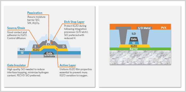
Figure 8. On the left is a traditional bottom-gate MOx TFT architecture; on the right is a self-aligned top-gate design. The topgate approach is better suited for 8K Gen10+ FPDs.
Yet another advantage is improved image quality. OLED displays can suffer from uneven brightness across their surface, caused at the transistor level by parasitic capacitance between a TFT’s gate electrode and its source/drain electrode. This parasitic capacitance can occur anywhere on the display and, as it fluctuates, it leads to varying levels of brightness in those areas.
Lowering parasitic capacitance is essential for higher image quality. One way to do so is with a self-aligned top-gate TFT architecture, which enables the gate and source/drain electrodes to be farther apart, reducing the potential for parasitic capacitance.
In addition, the amorphous IGZO (a-IGZO) TFTs used in displays feature an ES layer that protects the a-IGZO active layer from damage during etching of the source/drain electrodes. The ES layer ensures there is good contact between the source/drain and the channel, thereby reducing the high parasitic capacitance that can occur there and decrease the operating speed of the TFT circuit.
NEW CAPABILITIES FROM APPLIED MATERIALS
The Applied Materials Display and Flexible Technology group has successfully scaled up PVD and CVD tools for G10+ FPD production (figure 9). Applied Materials helps Gen10+ display manufacturers accelerate yield ramps with best-known methods (BKMs) for thin-film processing and inspection, achieve quick recovery from yield excursions with in-line scanning electron microscopy (SEM), and enable higher yield entitlement with superior thin-film architectures.
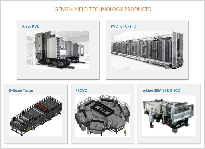
Figure 9. Applied Materials offers a wide array of capabilities for Gen 10+ FPD production.
Applied’s Gen10+ capabilities include:
- Highly differentiated rotary cathode PVD technology with maglev glass transfer to provide superior particle control for Gen10+ production.
- CVD solutions featuring hollow-cathode gradient and plasma confinement for integration of IGZO backplane technology.
- Scale up of Applied’s state-of- the-art inline SEM review tool to Gen10+ glass sizes. First used in integrated circuit fabrication, SEM technology is transitioning to the display fab to drive rapid yield entitlement (i.e., to maximize yield in the shortest time during setup), and to minimize yield losses due to problems such as particles (figure 10).
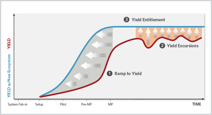
Figure 10. Applied Materials Gen10+ production tools help display manufacturers accelerate yield ramps, achieve quick recovery from yield excursions, and enable higher yield entitlement with superior thin-film architectures.
CONCLUSION
Display manufacturers are racing to set up fabs to produce the world’s most advanced TV display technology: 8K Gen10+ FPDs. High yields are essential to produce these products in volume at high margins, and Applied Materials’ proven deposition technology is a key to achieving those high yields.
For additional information, contact kerry_cunningham@amat.com.