Products & Technologies
Products & Services
Contact
Back to Menu
Products & Services
Products & Technologies
Services
Resources
Contact
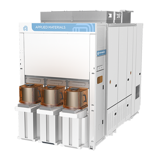
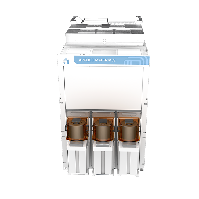
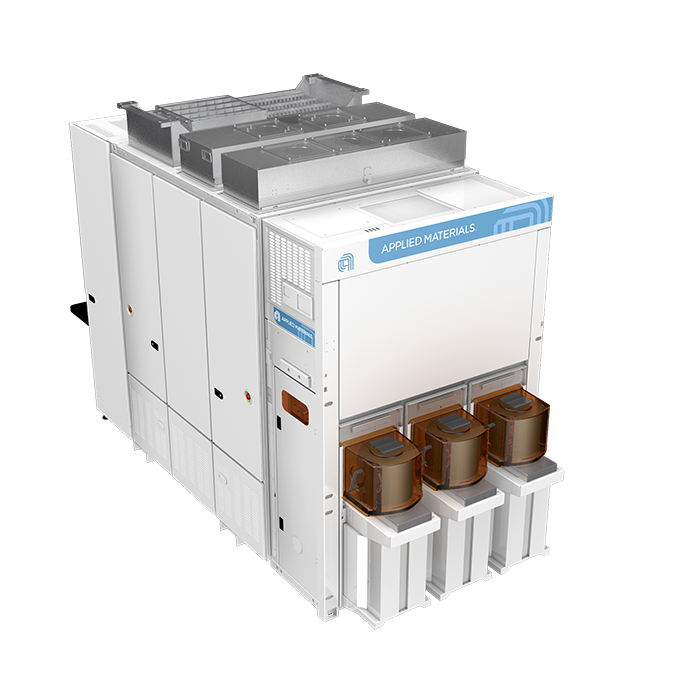
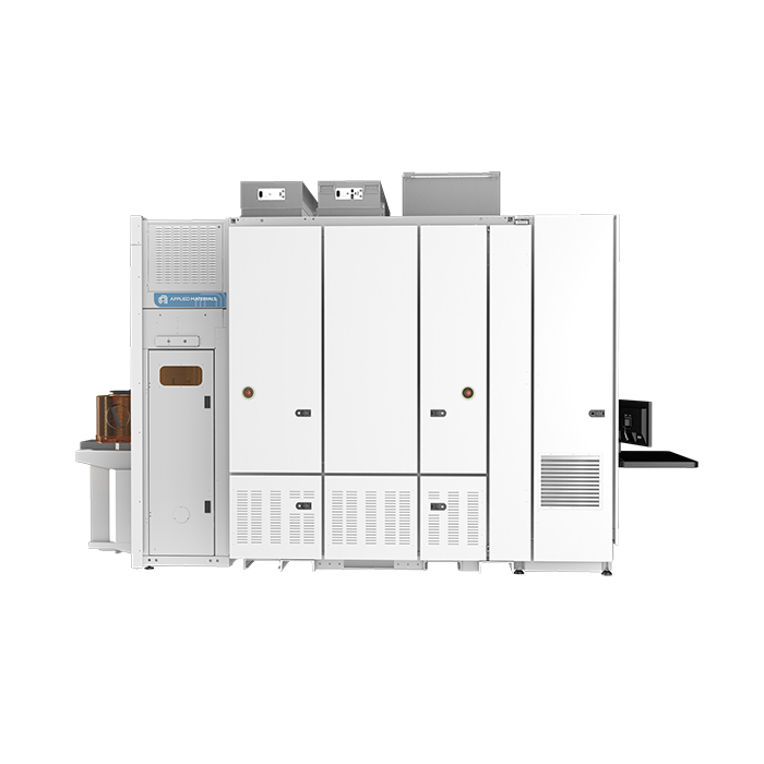
HawkEye Optical Inspection
As chip structures become ever smaller and processes grow in complexity, more inspection steps are required to enable effective process control. At the same time, fabs need to control costs, which is why they must deploy an approach that optimizes the total cost of inspection. A mix and match of optical inspection techniques–both brightfield and darkfield–is the key for cost-effective yield monitoring and control. The ultimate goal is to detect all key defect types in every critical process step so a fab can identify and fix issues early in development and ramp to high-volume manufacturing with higher wafer yield and reliability.
The HawkEye™ optical inspection system is used to inspect patterned wafers for darkfield defects–including particles, pattern defects, scratches, and humps–after etch, CMP, deposition, lithography, ion implantation and a variety of custom process modules. A deep ultraviolet (DUV) laser source provides high sensitivity and high throughput when scanning the fins, gate-all-around layers, and interconnect layers of memory and logic chips down to 2nm and a wide range of devices found in ICAPS– IoT, communications, automotive, power and sensors –markets. The HawkEye optical system’s lower cost of ownership helps keep overall inspection costs low while also allowing for more inspection points that lead to higher yield and reliability.
The HawkEye optical system is designed to maximize inspection throughput and detect all surface defects on patterned front-end-of-line, middle-of-line and back-end-of-line layers. It complements the Applied Materials Enlight™ brightfield optical inspection system, allowing fabs to pursue a comprehensive brightfield and darkfield inspection strategy.
- 1 / 4
- 2 / 4
- 3 / 4
- 4 / 4