Products & Technologies

Products & Services
Company
Contact
Back to Menu
Products & Services
Products & Technologies
Services
Resources
Company
Contact
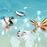
BUILDING A SUSTAINABLE SUPPLY CHAIN FOR A BETTER FUTURE
By Gary Dagastine
Applied Materials’ efforts to build a robust and sustainable supply chain for semiconductor and display manufacturing received increased focus earlier this year when the company announced its Supply Chain Certification for Environmental and Social Sustainability initiative (SuCCESS2030).
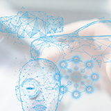
PHOTONIC DEVICE TECHNOLOGIES FOR EMERGING MARKETS
By Shiva Rai
Photonic devices such as lasers, photodetectors, microLEDs, and photonic-integrated-circuits (PICs) are the building blocks for new technologies, including facial recognition, 3D sensing, and laser imaging, detection and ranging (LiDAR).
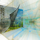
OLEDS: DISPLAY'S NEXT BIG THING
By Kerry Cunningham
After years of hope and promise, the adoption of large-area OLED displays for televisions, laptops and computer monitors is finally beginning to happen.
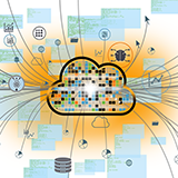
CONTROL AND DIAGNOSTICS INNOVATION IN THE “NEW NORMAL”
By David Lammers
The Covid-19 pandemic has accelerated collaborative-while-remote development in the semiconductor industry because travel restrictions and improved cloud security have encouraged more semiconductor fabs to allow controlled visibility into fab data, according to participants at the Advanced Process Control and Smart Manufacturing (APCSM) 2020 Conference, held virtually in early October.