Products & Technologies

Products & Services
Company
Contact
Back to Menu
Products & Services
Products & Technologies
Services
Resources
Company
Contact
Photonic Device Technologies for Emerging Markets
By Shiva Rai

Photonic device technologies have long existed for applications such as laser scanning and printing, telecommunications, and industrial material processing. More recently, light-emitting diode (LED) lighting has seen mass adoption. Photonic devices such as lasers, photodetectors, microLEDs, and photonic-integrated-circuits (PICs) are the building blocks for new technologies, including facial recognition, 3D sensing, and laser imaging, detection and ranging (LiDAR). To meet today’s application requirements, innovative device architectures, new materials development, monolithic and heterogeneous integration of materials, larger wafer sizes, and single-wafer processing are required for these technologies.
Introduction
Silicon (Si) has been the backbone of all the semiconductor IC technologies that have enabled the electronics evolution from computers to the Internet to smartphones, and now artificial intelligence (AI) and 5G. However, for certain applications, photonic device technologies are better suited to meet technological and environmental requirements.
Compound semiconductors, such as gallium arsenide (GaAs), indium phosphide (InP), and gallium nitride (GaN), have a direct-energy bandgap that enables photonic device technologies such as lasers and LEDs. Single-mode lasers at 1.3µm and 1.5µm using indium gallium arsenide phosphide (InGaAsP) materials have created very efficient fiber-optic communication systems in use today.
With the technological advancements made in GaAs- and GaN-based visible LEDs, the lighting industry has produced efficient and high-brightness LED products for indoor and outdoor lighting, automotive lighting, and displays. Apart from energy efficiency, LEDs have given lighting designers greater degrees of freedom that, for example, can be observed in the latest automotive headlights (Figure 1).
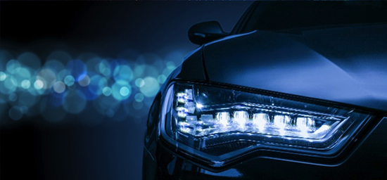
Figure 1. High-brightness LEDs have been adopted in recent automotive headlight designs.
EMERGING PHOTONICS APPLICATIONS
Photons are considered an important enabler of emerging technologies such as 3D sensing, autonomous vehicles, and optical interconnects. Just as electrons have been the backbone in designing the “brains” of machines, photons will supply “vision” for future machines. Laser will be the source of these photons.
3D Sensing
As smartphones are increasingly used for computing, more personal information is being retained on them, requiring stringent security beyond fingerprint and 2D iris scan for authentication. Vertical cavity surface emitting lasers (VCSELs) have lately attracted considerable attention in the consumer market after Apple introduced facial recognition in their 2017 iPhone X mobile device. The VCSELs shine tens of thousands of laser beams on the user’s face, which are then collected to produce a 3D depth map of the face, creating a unique identifier for that user (Figure 2).

Figure 2. VCSELs are the basis of facial recognition being used for device security.
The latest product from a leading consumer products manufacturer has extended this technology with a time-of-flight laser sensor that uses VCSELs to flash the scene a couple of meters away and create a 3D image of that space with depth information. For example, you can now virtually place a piece of furniture or artwork in a space to visualize it before purchase. For eye safety, the technology today is limited in wavelength range, but we can expect it to evolve to longer wavelengths in the future and to a broader variety of devices, including smartphones.
Optical Interconnects
Traditional data centers are consuming more than 2% of the world’s electricity today and global data traffic is expected to double every four years. In the future, data transfer between racks using electronic packet switches will not simultaneously meet the requirements for bandwidth and energy consumption. With the data center business model shifting to cloud computing, much greater volumes of data processing and transfer will be handled in coming years (Figure 3).

Figure 3. Cloud computing will exacerbate the challenge of data center energy consumption.
Si photonics and InP PIC-based optical interconnects are being developed to address these data center challenges. Transceiver modules at 100GbE are already in the market, with a steady push towards 400GbE and beyond. Si photonics enable faster data transfer over longer distances compared to conventional electronics, while utilizing semiconductor lasers and the efficiencies of high-volume Si manufacturing.
LiDAR
The next big paradigm shift in the automotive industry, besides electrification, is autonomous driving. For today’s Level 3 autonomy, very sophisticated illumination, detection, perception, and decision-making systems need to work together seamlessly (Figure 4). LiDAR has been widely accepted as the best solution for autonomous driving given its high-resolution, 3D imaging capability and achievable range beyond 200m that distinguish it from either radar- or camera-based solutions.
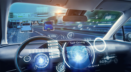
Figure 4. Safe operation of autonomous vehicles requires seamless coordination of many different systems.
The two frequency options for LiDAR are 905nm and 1550nm, with 905nm being preferred due to the well-established ecosystem for lasers and photodetectors. However 1550nm is being actively researched given its longer range and 40x higher eye safety limit compared to 905nm. Beam-steering technologies being evaluated include mechanical rotation, MEMS, and optical phased arrays. While a mechanical rotation presents significant reliability concerns, MEMS-based beam-steering technologies are featured in several recent car models as a Level-3 advanced driver-assistance systems (ADAS) option, despite limitations in range and field-of-view. Solid-state optical phased arrays for beam steering are in early development but hold promise in performance, cost, and form factor that could find future applications beyond autonomous driving. To meet the cost and performance requirements of the LiDAR system, heterogeneous integration or co-packaging of lasers, detectors, and beam-steering chips in high-volume manufacturing is needed. Today, MEMS-based LiDAR technologies are showing great promise for satisfying these industry requirements.
MicroLEDs
Apart from achieving higher resolution in existing devices such as TVs, smartphones, and smartwatches, microLED technology can potentially enable new and exciting products such as augmented reality/virtual reality (AR/VR) as illustrated in Figure 5. These new applications demand self-emissive red-green-blue (RGB) displays rather than color conversion or filtering. The challenges involved here are achieving required quantum efficiencies from RGB microLED die, cost-effective mass transfer of microLEDs onto the backplane, and testing of each individual microLED. Innovative device designs, epi growth optimization, substrate engineering, die transfer methodologies, and new backplane architectures are being investigated and developed to make microLED technology competitive with incumbent liquid crystal display (LCD) and organic LED (OLED) technologies.
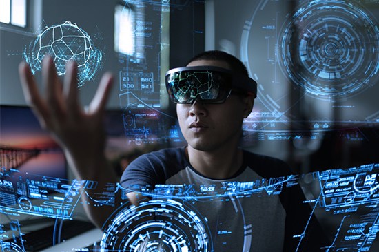
Figure 5. AR/VR applications are among the consumer products benefiting from microLED technology.
DEVICE TECHNOLOGIES
The key device technologies enabling these emerging photonic applications are GaAs- and InP-based lasers, Si and indium gallium arsenide (InGaAs) photodetectors, MEMS devices, GaN and GaAs LEDs, Si and silicon nitride (SiN) waveguides, and optical modulators. For 3D sensing applications, GaAs laser devices are shifting from 100mm to 150mm substrates. GaAs and GaN LEDs used in high-brightness applications are in production on 150mm GaAs and sapphire substrates, respectively. However, microLED applications are driving the demand for RGB LEDs on Si substrates in certain applications. InP laser diodes are manufactured on 75mm and 100mm InP substrates. Compound semiconductor devices are typically processed in batch reactors, but manufacturing focus is growing on improving yields, within-wafer uniformity, and process control. Consequently, there is a push to transition to single-wafer processing tools.
MEMS devices used in beam-steering technologies currently depend on 200mm Si MEMS production lines. Si photonic technologies are predominantly run on 200mm silicon-on-insulator (SOI) platforms with a constant push to transition to 300mm wafers to address technological limitations in 200mm tools, e.g., lithography and etching. Thin-film technologies with high electro-optic coefficients are constantly being investigated to extend the speed and bandwidth envelopes of optical interconnects.
The photonic applications discussed here are forecast to have a tremendous growth trajectory over the next 5–10 years. The four key applications—3D sensing, LiDAR, optical interconnects, and AR/VR displays—collectively are forecast to grow from an $8B market in 2020 (Figure 5). AR/VR applications are among the consumer products benefiting from microLED technology to $23.3B in 2025 at a CAGR of 31% (Figure 6). While 3D sensing technologies are finding new applications, LiDAR and AR/VR displays are at early development stages and are expected to grow at much higher CAGRs. The growth in photonics applications will require addressing device technology challenges in performance, manufacturing, and system-integration. Today forces are driving demand for new process equipment that can not only resolve device performance challenges but also deliver superior process control and improve overall manufacturing yields.
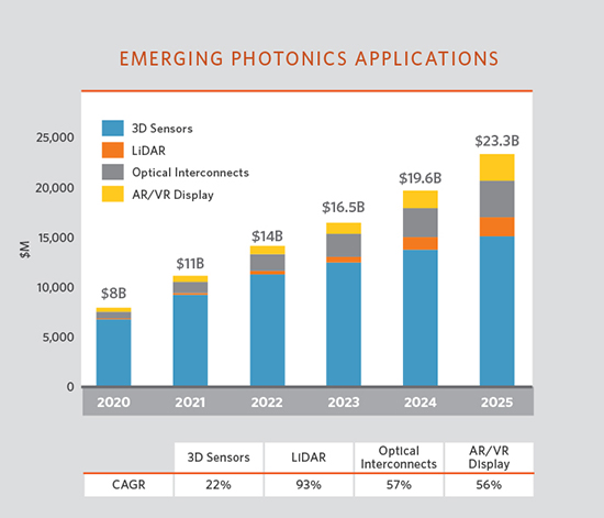
Figure 6. Emerging photonic applications have tremendous growth trajectory. (Source: Yole Développement reports)
Shiva Rai is Strategic Marketing Manager for Photonics & RF applications at Applied Materials. For additional information contact him at shiva_rai@amat.com

Shiva Rai, Strategic Marketing Manager for Photonics and RF Applications