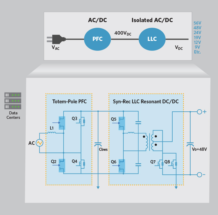
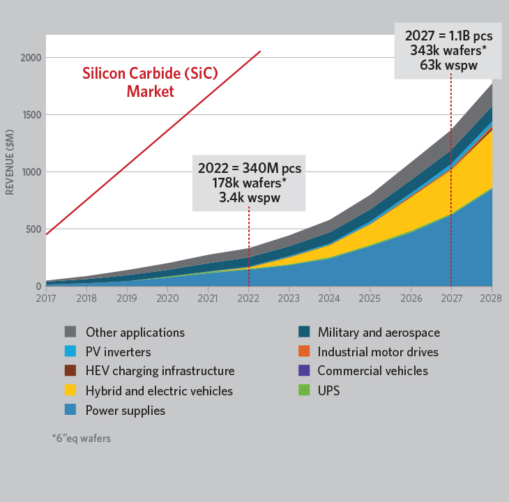
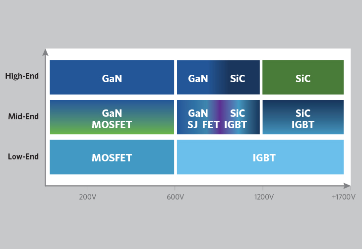
Figure 3. GaN is suited for high-frequency power supplies, while SiC is appropriate for applications requiring higher power and robustness, such as motor drives and industrial power. As WBG devices become better established in the market, technology adoption will become more defined. (Source: Yole Développement)
GaN DEVICE MANUFACTURING CONSIDERATIONS
Each process involved in manufacturing GaN HEMTs must be very precise to achieve the best device performance and reliability. The fast switching, high power density, and high voltage breakdown of WBG devices demand extremely high-quality epi layers and dielectric deposition with precise etching and metal deposition.
MOCVD
MOCVD is critical in creating the GaN device as it grows the various epi layers above the substrate. Defect density, within-wafer uniformity, and wafer-to-wafer repeatability are key considerations in MOCVD development, especially when transitioning to 200mm. Given the different lattice constants and thermal coefficients during expansion of GaN and silicon, growing epitaxial GaN on silicon to create stable and reliable HEMTs is a challenging process in super lattice structures and stress management.
Etch
Etching is also a critical process in manufacturing GaN devices. Two notable challenges are the high selectivity of GaN/AlGaN and the potential for an over-etch on the AlGaN from the p-GaN etch to cause roughness on the surface, which reduces sheet resistance. Additionally, HEMTs with recessed gates require a certain AlGaN thickness, which must be well controlled and highly repeatable. Atomic-layer precision and advanced endpoint monitoring are essential.
CVD
The GaN HEMT structure typically has multi-layer field plates to minimize voltage peak stresses at gate-drain contact and dynamic RDS(on). Films such as SiO2 and SiN are used as dielectrics. These must be of the highest quality to minimize film contamination and reduce thermal degradation at elevated temperatures while improving film stoichiometry. In addition, film stress must be controlled to avoid wafer bowing. This can be achieved through RF power among other process parameters.
Surface passivation of SiN has been proven to improve two-dimensional electron gas conductivity by creating higher carrier concentration, which in turn improves device performance. Alternative materials, such as Al203, use atomic layer deposition to improve device performance.
PVD and Plating
GaN HEMTs are lateral devices with a very high current density, so most of the losses happen at the top of the die. In a normal discrete package, the bottom of the die would be attached to the copper lead frame. However, the silicon substrate has a relatively low thermal conductivity, which results in a higher operating junction temperature of the device. Operating too close to the maximum junction temperature adversely affects reliability and temperature-dependent characteristics such as RDS(ON). Therefore, it is crucial to promote heat transfer away from the die. Implant techniques that reduce the resistance of the ohmic contact help improve heat dissipation. Also, depositing thick copper on the top of the die increases thermal capacity and conductivity, while allowing for the possibility of sintering copper lead frames and clips. This improves reliability in power cycling and significantly reduces mechanical stress resulting from mismatched coefficients of thermal expansion.
CONCLUSION
As energy demands rise, the search for greater power efficiency is spurring growing interest in GaN as a successor to silicon semiconductors in high-power, high-efficiency applications such as adaptors, 5G, data centers, and electric vehicle chargers. However, manufacturing GaN devices demands exceptional film quality and a high degree of process precision in epitaxy, dielectric and metal deposition, and etch. While its market was very limited before 2019, GaN is now taking hold in travel adaptors, with automotive and data center applications expected to follow once the reliability of the technology has been firmly established.
For additional information, contact llew_vaughan-edmunds@amat.com


