Products & Technologies

Products & Services
Company
Contact
Back to Menu
Products & Services
Products & Technologies
Services
Resources
Company
Contact
Enhanced Tault Detaction Comes to Semiconductor Assembly, Test and Packaging
By Chris Reeves and Ben Williams
Applied Materials’ new Applied SmartFactory® Fault Detection solution offers an economic, easy-to-implement way to improve tool and process performance in the back end.
Wafer fabs have long embraced factory automation solutions because they enable users to improve yield and output, reduce cycle times and costs, and increase profitability by leveraging the vast amount of data in front-end semiconductor operations.
However, back-end assembly, test, and packaging (ATP) operations have been challenged in implementing automation given a history of manual operation, use of legacy equipment and nonstandard data protocols, and lack of a suitable platform for comprehensive data analysis.[1]
But data volumes and velocities are now surging in the back end as well, prompting ATP factories to turn to automation. Fault detection (FD) is often the initial focus because it doesn’t require an extensive investment and factory overhaul, yet it can provide much more granular detail about equipment and product health.
DRIVERS OF CHANGE
Several factors are driving the data explosion in ATP. The desire to achieve high yields is a key one, because of their impact on profit margins. By the time a wafer reaches the assembly/test phase of production, significant resources have been invested in it and the cost of scrap is high. An enhanced ability to work with data to discover and prevent faults is vital to achieving yield targets.
Another factor is the growing demand for higher-quality production as the use of chips in automotive and other applications increases. Many of these applications also require ATP suppliers to document the origin or production history of their output (e.g., wafer history, die tracking, and shipment tracking) to certify that it meets customer industry standards. This requirement is a formidable challenge because multiple chips can reside within the final packaged product, and those chips typically come from different wafers and different lots. Consequently huge amounts of data must be collected, analyzed, and preserved to document everything adequately.
Additionally, in recent years the ATP sector has expanded its capabilities and scope of services, creating increased work output and faster work flows—along with greater volumes of data. For example, with just one wire bonder literally hundreds of touch points/sec must be captured, stored, and analyzed, resulting in a large data set from just that single tool.
Figure 1 gives an overall perspective of data rates in the back end. To capture all the data points needed to fully characterize back-end tools and processes at an average data rate of 824.13 Hz/tool, the data flow is estimated to be 0.5 GB/sec. That amounts to 30 GB/min, 1,833 GB/ hour or 44,000 GB/day! Retaining this much data for 90 days would require ~4 petabytes of storage, equivalent to ~20,000 billion pages of typed text. Clearly, existing back-end data management systems are inadequate to handle this data volume.
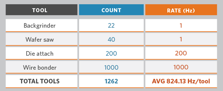
Figure 1. Data rates are surging in the back end.
FURTHER COMPLICATIONS
While front-end semiconductor fabs have been using FD and automation to address data challenges successfully, their adoption in ATP operations has been much slower because the issues in this sector are substantively different. Key issues include data complexity and volume, lack of data communication standards, and inadequate data retrieval speeds.
In the semiconductor front end, most equipment complies with the SECS/GEM equipment-interface standard. But in the back end, other data protocols are also commonly used, such as log files and the Open Platform Communications Unified Architecture (OPC UA) machine-to-machine communications protocol. Historically, ATP manufacturers have addressed the lack of data communication standards through proprietary methods. However, as industry demand for higher-quality production increases, many have begun looking to third parties for more robust solutions.
Additionally, ATP data exists in many forms with no common platform for analysis. This gives rise to complexities, gaps, and delays in data collection, as well as analysis and storage/retrieval challenges. An example is when a tool’s trace inputs (i.e., sensor data describing critical process parameters) are stored in OPC servers, but the contextual information that describes the product being manufactured by that tool is located in a separate system in a log file format.
Further adding to the complexity is the nonstandard structure of log files. Although log files theoretically can be used to store both tool sensor data and contextual information, any given log file’s structure is determined by the equipment manufacturer and may be implemented in a proprietary fashion.
Finally, as aging tools are upgraded (usually by adding external sensors), ATP operators frequently develop proprietary data-collection architectures. OPC servers may be used as a central location for data storage, but the data they contain may represent just a portion of the overall picture of a tool. And in any case, OPC offers no capability to analyze, model, and act on the data collected.
APPLIED’S NEW FAULT DETECTION SOLUTION
Applied Materials developed its new SmartFactory Fault Detection solution, now in beta testing with customers, as a fast, cost-effective way to propagate front-end FD practices into back-end ATP operations.
Built on the company’s mature and widely deployed Applied E3® advanced equipment and process control technology, the new solution incorporates a customized version of the kdb+[2] relational time-series database. This database is commonly used in the finance industry for high-frequency trading and in many industrial applications where it is vital to have the ability to capture and work with time-based data when ordering events in large data sets at high speed.
The SmartFactory Fault Detection solution helps customers build a complete data picture of their operations. It collects data from OPC servers, tool log files, and other factory data sources to monitor and improve wafer quality; provides a multidirectional look into these sources beyond what is available in standard tool interfaces; improves data access/processing speeds for better engineering efficiency and effectiveness; and provides ease of data retrievability beyond standard runtime windows of 60, 90, and 180+ days. See figure 2.
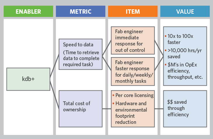
Figure 2. The benefits available from the kdb+ time-series database that Applied Materials has incorporated into its new SmartFactory Fault Detection solution.
The kdb+ database has RAM-based in-memory capabilities for fast data storage/retrieval. It also has a column-based data structure and proprietary query language, allowing for optimized database queries with no need to export data to other applications for analysis. See figure 3.
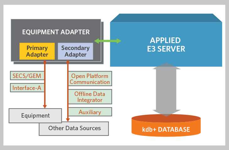
Figure 3. Schematic of the architecture of the new SmartFactory Fault Detection solution. In internal use at Applied, queries that otherwise would take 10+ minutes to complete have been returned in <90 seconds.
AUTOMOTIVE QUALITY IS CRITICAL
One example of the benefits that can be achieved with Applied’s new SmartFactory Fault Detection solution comes from the automotive industry. The move toward autonomous vehicles is dramatically increasing the use of sensors and data processing, resulting in higher reliance on an uninterrupted supply of high-quality semiconductors.
Given the automotive industry’s tightly integrated supply chain and just-in-time practices, supplier quality lapses that could have been reasonably accommodated not too long ago now have the potential to cause great disruption. A case in point: In 2019, a quality lapse in a small but critical component used in electrically assisted steering systems caused automaker BMW to temporarily limit its production of 1-, 2-, 3-, and 4-series luxury cars. The quality lapse disrupted production at four BMW plants on three continents and had a significant financial impact on the company.
Moreover, automotive quality demands will only increase as the industry drives relentlessly toward its goal of a zero-failure rate. While a failure rate of 1 ppm in a semiconductor component is terrific for a desktop application, when you consider that there are ~50 automotive applications in a vehicle and that a typical automotive application contains ~400 components, the overall failure rate due to semiconductor quality rises to 20,000 ppm or 2% in total—far from zero!
Back-end process control systems that incorporate FD, such as Applied’s SmartFactory Fault Detection solution, along with an integrated platform will help ATP factories ensure and increase product quality by helping them detect problems earlier and at their source, eliminating process noise, and enabling statistical process control.
CONCLUSION
There is a growing imperative that back-end semiconductor ATP facilities be able to quickly and accurately identify issues in the production process, and then immediately correct them.
Applied’s new SmartFactory Fault Detection solution will help ATP customers achieve these objectives, while providing them an opportunity to achieve lower costs and higher margins.
[1]https://blog.semi.org/technology-trends/automated-material-handling-for-semiconductor-assembly-and-test
[2] kdb+® is a registered trademark of Kx Systems, Inc., a subsidiary of First Derivatives plc.
For more information contact christopher_reeves@amat.com and ben_williams@amat.com.

Chris Reeves, Global Product Manager for SmartFactory Fault Detection

Ben Williams, Senior Manager for Total Product Support