Products & Technologies

Products & Services
Company
Contact
Back to Menu
Products & Services
Products & Technologies
Services
Resources
Company
Contact
TABLE OF CONTENTS
AI Will Enable Next-Generation Quality Systems
Applied and SC Solutions Partner on Real-Time Profile Control for 200mm CMP
Foldable Phones Bend the Limits of Technology
Subject Matter Expertise is Critical for Smart Manufacturing Analytics
The Future of Power Needs to be Exotic
The Future of Power Needs to be Exotic
By Llew Vaughan-Edmunds
Moore’s Law follows the continual advancement of smaller silicon transistors, which is ideal for faster operating speeds in processors and increasing memory size density.
However, not all solutions require smaller transistors, and not all are made on silicon wafers. LEDs are made from gallium arsenide (GaAs) and lasers use indium phosphide (InP), while power devices are transitioning to silicon carbide (SiC) and gallium nitride (GaN) for better performance. These exotic materials deviate from silicon properties and provide superior performance with higher reliability.
A FASTER, SMARTER WORLD
Electronic equipment is becoming smarter: smartphones are scanning faces for identification and moving into augmented reality (AR) applications. Electric vehicles (EVs) are learning how to become autonomous through sensors and cloud computing, while maximizing battery life between each charge. The Internet of Things (IoT) is connecting everything and everyone, from house thermostats knowing their owners’ whereabouts, to distribution warehouses tracking packages in real time.
All this extra data will need to be transferred quickly using the 5G cellular network as the communication backbone. 5G is like pressing the light-speed switch, enabling download of a two-hour movie in three seconds, compared to six minutes on a 4G link.
This increased demand for more data, faster communications, and wider connectivity brings along an exponential increase in power requirements.
NEW REVOLUTION IN SEMICONDUCTORS
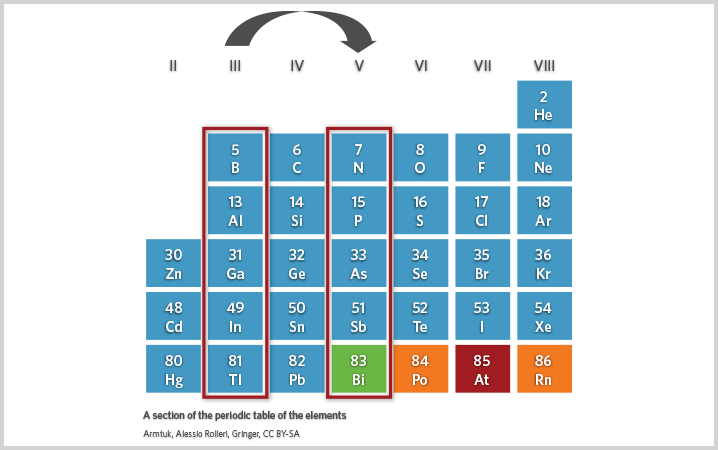
Figure 1. Gallium arsenide (GaAs), gallium nitride (GaN), and indium phosphate (InP) are compounds created from groups III-V, which enable high carrier mobility and direct energy gaps, ideal for emitting/receiving light and switching at radio frequencies <60GHz. (Source: Armtuk/Alessio Rollen, Gringer)
Silicon has been the work horse for over 50 years, but we now see the growth of compound semiconductors which support possibilities that silicon cannot provide (figure 1). These materials combine two or more elements, and allow electrons to flow much faster, in some cases supporting processing speeds 100 times faster than silicon. They emit and sense light, generate microwaves, are sensitive to magnetism and are resistant to heat. They do all this and use only a fraction of the energy of a silicon-based solution.
These materials never went into serious volume production over the last 30 years due to challenges in manufacturing, such as compound crystal growth, high defectivity, and breakability. The cost and complexity were simply too much to compete with silicon-based solutions.
More recently, however, compound semiconductors have advanced as high-volume production, continuous material improvements, and new processes combine to bring down costs to levels where customers are starting to accept them over silicon. As higher-end solutions such as those for EVs or 5G emerge, requiring levels of performance that silicon cannot achieve, system designers increasingly are choosing compound semiconductor-based devices, and the extra cost becomes justifiable.
NEED FOR SPEED
All smartphones and wireless communication systems transmit and receive signals in the radio frequency (RF) spectrum. To convert an electrical signal to a radio frequency, RF amplifiers are needed. These use a range of III-VI materials including GaAs, GaN, and InP devices.
The main advantages of 5G are superfast data rates (<10 Gps), ultra-low latency (<1 ms), and highest reliability (~99.99%)—all demanded by a data-hungry society seeking fast movement of data to the cloud, reliable live video streaming, AR/VR, and the fast response times required for the IoT and autonomous transportation.
Currently the main power switches for RF communications are made on silicon (often a laterally diffused MOSFET [LDMOS] process) and GaAs. However, as 5G frequencies go to 100 GHz, these materials start to lose steam. Silicon LDMOS cannot run higher than 3.8 GHz, therefore GaN-on-SiC will start to dominate this higher frequency and power band, typically focused on base stations. GaN-on-SiC supports very high-power densities, about 5X the power output compared to its GaAs counterparts, which makes GaN-on-SiC ideal for smaller solutions at the same power levels or for higher power levels at the same size (figure 2).
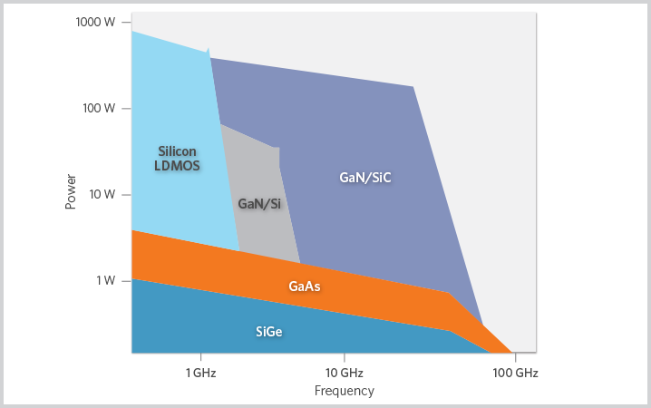
Figure 2. GaAs metal-semiconductor field-effect-transistors (MESFETs) are limited to low power, while GaN-on-SiC high-electron-mobility transistors (HEMTs) offer both high frequency and high power. (Source: Analog Devices)
As 5G ramps into high volume in the next years, the amount of amplification will exponentially increase. Micro cells, massive multiple-input and multiple-output (MIMOs[1]), and beam forming are just some of the new infrastructure that 5G will require to provide reliable levels of signal and bandwidth (figure 3).
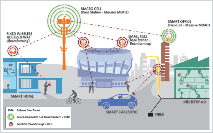
Figure 3. 5G is expected to have download speeds of 10 Gbps, more than 1000x faster than 4G. A completely new infrastructure will be required to effectively transmit and receive that level of data reliably. (Source: Infineon Technologies)
Currently 5G requires approximately 4X more system power than 4G, and the additional power requirements—beyond what is possible with GaAs solutions—make GaN-on-SiC increasingly attractive.
CARS GET CLEVER
The evolution to self-driving cars is in full swing, though it will probably take a decade or more to pass legislation before we start seeing them in volume on the roadways. There are five levels of autonomy, where Level 5 is a completely self-sufficient, driverless, car.
Currently the industry provides support for Level 2 functions, such as emergency steering, acceleration and braking functions, using multiple data sources. These advanced driver-assistance systems (ADAS) are designed to increase road safety and enable autonomous driving (figure 4).
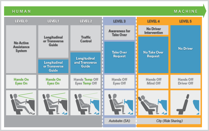
Figure 4. Levels of human vs. machine driving control. To become autonomous, the car needs to key where it is going, what is around it, and what to do in every possible scenario. (Source: http://www.businessinsider.com)
For the car to have “vision,” a number of possible technologies are being developed, such as image cameras, radar, light detection and ranging (LiDAR), and ultrasonic sensors. All have their advantages and disadvantages, and it is likely that cars will instead incorporate a “sensor fusion” approach, combining two or more of these technologies (figure 5).
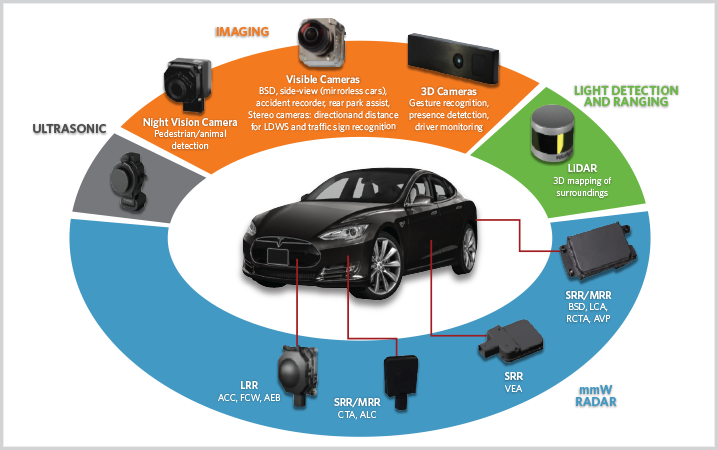
Figure 5. A number of mechanisms will likely be combined to provide vision functions in autonomous cars. (Source: Yole Développement)
LiDAR
LiDAR systems are designed to measure the distance to a target, using lasers to pulse light and a sensor to measure the reflected pulses. The pulsed lasers are typically rotated 360 degrees to create a 3D image of the surrounding area.
GaAs and InP laser diodes are the current choice today, depending on the range (figure 6). These lasers require high pulses of surge current at a very fast frequency. Today’s silicon MOSFETs are not able to provide that level of performance, therefore GaN high-electron-mobility transistors (HEMTs) are now the preferred choice. They can switch 10X faster with less noise than silicon transistors, providing superior resolution and faster response times.
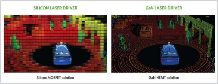
Figure 6. GaN HEMTs are necessary to provide high-resolution imaging for LiDAR by enabling high surge currents at fast frequencies. (Source: EPC Corporation)
TRACTION INVERTERS
Electrical motors have existed for over 150 years, and there are many types optimized for different applications. For EVs, typically an AC induction motor or permanent magnet motor is used. Permanent magnet motors have higher efficiency and power density, but are more expensive to manufacture than induction motors.
Most industrial motors today use insulated-gate bipolar transistors (IGBTs) co-packed with a diode, however IGBTs are minority-carrier devices which behave similarly to a bipolar transistor by injecting holes into the drift region. While this is good for lowering resistivity, it increases switch-off time due to the recombination of minority carriers. This leads to higher switching losses due to slower tail current recovery. SiC MOSFETs are majority-carrier devices which have no discernible recovery time and transition significantly faster. This leads to lower power losses and higher system efficiency (figure 7).
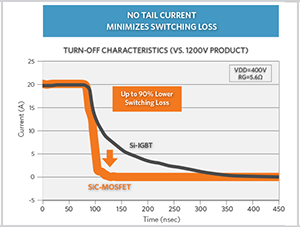
Figure 7. Compared to conventional silicon IGBTs that utilize a high-voltage switching element, SiC devices can reduce the power lost during switching by over five times. (Source: ROHM Corporation)
Tesla was among the first EV makers to use SiC devices in the traction inverter. SiC solutions will provide an estimated 10-15% additional mileage range, which makes SiC attractive for longer range EVs (figure 8).
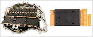
Figure 8. Tesla Model 3 traction inverter showing the SiC MOSFET power modules from ST Microelectronics.
DEVICE PRODUCTION OF SiC/GaN
SiC is a very hard material that requires special tooling and technologies for grinding, dicing, etching, and implanting. Typically, higher energies and higher temperatures are needed to manipulate the material characteristics.
Also, GaN-on-Si and GaN-on-SiC need precise layers of material stacking to ensure good lattice alignment, a buffered coefficient of thermal expansion between the GaN and the substrate, and the lowest-charge trapping between interface materials.
Applied Materials has a selection of released and in-development technologies to support the processing of wide bandgap (WBG) materials, such as high-throughput CMP, deep reactive ion etch (DRIE), high temperature implant, and deposition.[2]
One of the main considerations was the handling of SiC wafers. These are transparent wafers that current sensors are not able to detect. Therefore, a completely new approach and system kit was required to handle these types of wafers (figure 9).
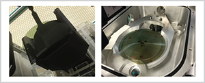
Figure 9. Endura PVD wafer mapping and orientating a 150mm SiC wafer. (Source: Applied Materials)
CONCLUSION
The evolution of end systems is changing to become faster, smarter and more autonomous. This has energized the need for extra sensors, faster data transmission and significantly more power. Compound semiconductors such as GaAs, GaN, and SiC have now become one of the fastest growing markets for the foreseeable future, as 5G and EVs hew a path toward a new landscape.
Llewellan Vaughan-Edmunds is Director of Strategic Marketing for Power Technologies in Applied Materials’ newly formed ICAPS group, which is focused on enabling MtM technologies through the development of new materials and unit processes delivered via Applied Materials production toolsets on 300mm (≥28nm) and ≤200mm wafer sizes. For additional information contact him at llew_vaughan-edmunds@amat.com.