Products & Technologies

Products & Services
Company
Contact
Back to Menu
Products & Services
Products & Technologies
Services
Resources
Company
Contact
TABLE OF CONTENTS
AI Will Enable Next-Generation Quality Systems
Applied and SC Solutions Partner on Real-Time Profile Control for 200mm CMP
Foldable Phones Bend the Limits of Technology
Subject Matter Expertise is Critical for Smart Manufacturing Analytics
The Future of Power Needs to be Exotic
Big Data Analytics for Smart Manufacturing
EQUIPMENT AND PROCESS EXPERTISE ARE CRITICAL COMPONENTS OF ANALYTICAL SOLUTIONS FOR SEMICONDUCTOR MANUFACTURING.
By James Moyne and Jimmy Iskandar
Applied Materials has led the way over the past few years in determining a big data analytics path for the semiconductor manufacturing industry. In addition to supporting premier technical conferences such as the US, Asia and Europe APC Conferences,[1] Applied’s work has been validated through publication in peer-reviewed journals such as IEEE Transactions in Semiconductor Manufacturing.[2] One such article, published in Switzerland-based MDPI’s open access journal Processes, received the Best Paper Award 2016 and 2017.[3] It explored trends and opportunities in big data analytics in semiconductor manufacturing, and provided a roadmap for adopting analytics to support applications ranging from fault detection to predictive maintenance. High points of the article[4] are presented here.
SHAPING OUR SMART MANUFACTURING ANALYTICS VISION
Smart manufacturing (SM) is a term generally applied to a movement in manufacturing practices toward integration up and down the supply chain, integration of physical and cyber capabilities, and use of advanced information for increased flexibility and adaptability. SM leverages the tremendous advances in volume, velocity, variety, veracity (i.e, data quality) and value (analytics) of data, often referred to as “big data,” by applying big data analytics to improve existing analysis capabilities and provide new capabilities such as predictive analytics. These improved and new capabilities, summarized in figure 1, are considered part of the extended advanced process control (APC) family.
The emergence and evolution of equipment- and process analytics for semiconductor manufacturing have been shaped in part by three key industry challenges. Figure 1. Definitions of APC and APC-extended capabilities. These challenges have existed for decades and are not specific to SM or the big data revolution; however, they are somewhat unique to semiconductor manufacturing. They are (1) equipment- and process complexity, (2) process dynamics and context richness and (3) poor data quality in terms of both accuracy and availability.
These challenges have resulted in the realization that analytics solutions for the semiconductor industry cannot be strictly data-driven. Tool, process and analytic domain knowledge, or subject matter expertise (SME), is also a critical component of most fab analytical solutions. Therefore, process analytics in the industry are, and will continue to be, designed and employed with this in mind. Indeed, often the mechanism for SME input is formally defined in areas ranging from data collection, data treatment, parameter selection, model building, model and limits optimization, and solution deployment and maintenance.
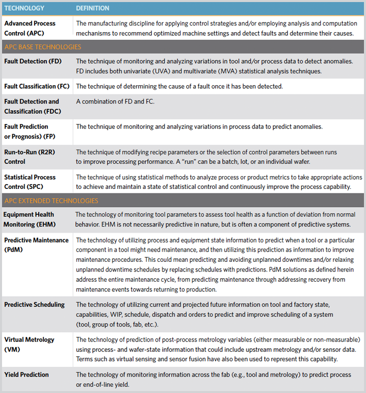
Figure 1. Definitions of APC and APC-extended capabilities.
UNDERSTANDING THE COMPONENTS OF SEMICONDUCTOR MANUFACTURING ANALYTICS
There has been an explosion in analytical approaches over the last decade, and many have been developed to take advantage of the promise of big data. One way to identify and categorize these analytics is to define dimensions of capability in analysis and specify or plot analysis capabilities with respect to these dimensions. Figure 2 provides a breakdown of dimensions relevant to analytics in semiconductor manufacturing.
Given these dimensions, an analytic application or analysis can then be defined with respect to the value the capability has in each dimension. For example, an analytic, principal component analysis (PCA)—often used in multivariate analysis (MVA), fault detection (FD) and equipment health monitoring (EHM)—is unsupervised and reactive. MVA is generally static and stateless, and does not formally incorporate SME. With respect to analysis applications, FD in today’s fabs is largely unsupervised, reactive, univariate, stateless and statistically based, with SME incorporated in FD model development. Defining analytics and analysis applications using these and other dimensions provides a framework for identifying gaps in capability, opportunities for advancement, and over the longer term, roadmaps for improvement.
The recent evolution in APC applications for semiconductor manufacturing reflects a movement from a reactive to a predictive, and even a proactive, approach to factory control.[5] This relies heavily on the big data explosion, where support for larger volumes and longer data archives has somewhat enabled predictive solutions to decipher the complexities of multivariate interactions of parameters, characterize system dynamics, and reject disturbances and filter out data-quality issues.
In many cases the algorithms in these solutions must be rewritten to take advantage of the parallel computation afforded by big data solutions to process the data in a timely manner. New algorithms also may be developed that are more big data-friendly. For example, earlier predictive solutions relied on single-core CPU and serial processing, but with big data, partial least squares (PLS) and support vector machines (SVM) can be used for parallel computation on a server farm. Likewise, unsupervised data-exploration techniques such as self-organizing map (SOM) and generative topographic mapping (GTM) are rewritten to process large amounts of data, enabling users to quickly gain insights. Similarly, time-consuming statistical techniques such as hidden Markov model (HMM) and particle swarm optimization can be rewritten to become computationally far more efficient.[6]
However, a plethora of techniques and a massive amount of data do not necessarily lead to more insights and predictive capability. It is the authors’ belief that no one approach or combination of approaches is a panacea. Rather, approaches will be customized to applications given the data at hand. Nonetheless, we believe that SME will continue to guide the development and maintenance of solutions.
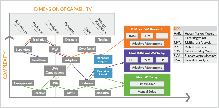
Figure 2. Dimensions of analytics capabilities, with mapping of typical semiconductor manufacturing APC solutions to these dimensions. Phenomenological models are physical model forms that represent process knowledge; they are tuned or modified with statistical data.)
THE EMERGENCE OF AI AND NEW BIG DATA-FRIENDLY ANALYTICS
The term AI can be used to describe any device or analytic that perceives its environment and takes action to achieve a goal. Today the term is often used to refer to the concept of devices or analytics mimicking the function of the human brain, as in self-driving automotive applications.[7] Artificial neural networks (ANN), an example of this type of analytic, have been around for decades and such AI analytics have resurged as part of the big data evolution. For example, deep learning, a technique very similar to structured ANN, leverages hierarchical abstraction for improved quality and speed of high-volume data analysis.
Deep learning can be utilized to address some higher dimensional problems in big data analytics, including extracting complex patterns from two-dimensional images (e.g., wafer maps).Deep learning techniques benefit from increased data volumes and use data-driven supervised techniques to find relationships in data. Their main drawback is their relative inability to incorporate SME in model development and maintenance.[8] The developed models are generally not explicitly available and as such are difficult to assess, while the context richness and dynamics involved in semiconductor manufacturing analysis hinder deep learning techniques from leveraging large and consistent data volumes. Recently research efforts have focused on combining SME with AI techniques, an approach that holds promise for future application on the manufacturing floor.[9]
Another big data analytical capability receiving significant attention is background analysis by solutions often termed as “crawlers.” [10] These applications mine data in the background, looking for patterns or analytical results of interest, such as a part nearing fault. They then asynchronously inform an application such as a factory control system so that appropriate action can be taken. This approach also allows diagnostics and prognostics to be more reconfigurable.
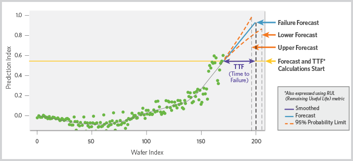
Figure 3a. PdM approach utilizing MVA predictor and its components, including time-to-failure horizon and some expression of prediction confidence or range.
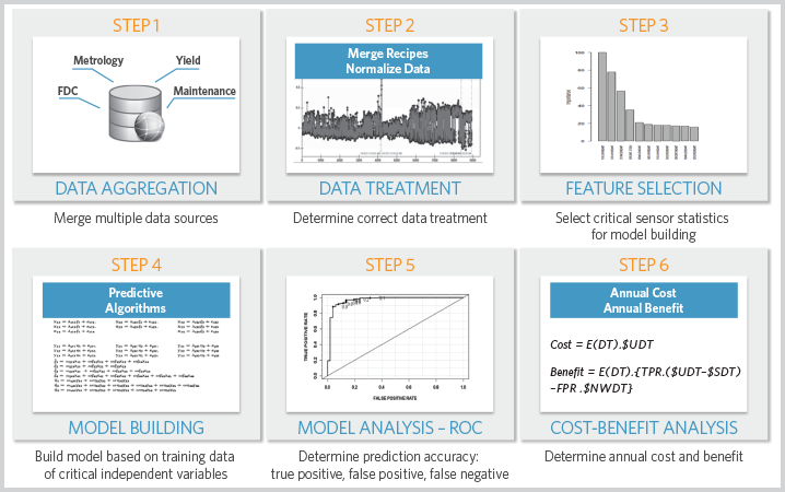
Figure 3b. PdM approach utilizing offline model building and optimization to provide a mechanism for incorporating SME that can be leveraged for many APC predictive capabilities.
LOOKING AHEAD: AN ANALYTICS ROADMAP
As we move towards SM, it is clear that analytics will continue to play a larger role in achieving yields while maximizing throughput and lowering cost. Big data advancements will power these analytics, and the authors believe that progress thus far has provided some key findings that will help maximize the power of these analytics.
The first of these is that many of the analytical solutions the industry is looking to develop or enhance can leverage the same model development (“data at rest”) and model execution/maintenance (“data in motion”) structure. For example, the 6-step model development process for PdM (summarized in figures 3a and 3b) can be used for virtual metrology or even for predictive yield. Leveraging a common approach will not only save time and effort in ramping these technologies, it also will enable manufacturers to cross-leverage the continuous advancement in analytical approaches.
The second key finding is that SM will allow the application scope of these analytics to be expanded. For example, extending diagnostics, control and prediction from the four walls of the fab into the supply chain will allow for better control to customer needs and enhance the ability to address problems such as field yield issues.
Third and perhaps most importantly, SME will continue to play an important role in analytics applications in our industry. Applications will vary, but equipment- and process expertise will remain critical components of analytical solutions for semiconductor manufacturing.

Jimmy Iskandar

James Moyne
For additional information, contact Jimmy_Iskandar@amat.com or moyne@umich.edu
[1] APC Conference US: https://www.apcconference.com; APC|M Conference Europe: https://www.apcm-europe.eu/home/; AEC/APC Symposium Asia https://www.semiconportal.com/AECAPC
[2] J. Moyne, J. Samantaray and M. Armacost “Big Data Capabilities Applied to Semiconductor Manufacturing Advanced Process Control,” IEEE Transactions on Semiconductor Manufacturing, Vol. 29, No. 4, November 2016, pp. 283-291.
[3]https://www.mdpi.com/journal/processes/announcements/1466
[4] J. Moyne and J. Iskandar, “Big Data Analytics for Smart Manufacturing: Case Studies in Semiconductor Manufacturing,” Processes, Vol. 5, No. 3, July 2017 Available online: http://www.mdpi.com/2227-9717/5/3/39/htm
[5] International Roadmap for Devices and Systems (IRDS): Factory Integration White Paper, 2018 edition. Available online: https://irds.ieee.org/
[6] An introduction to each of these algorithmic approaches can be found on Wikipedia: https://en.wikipedia.org/wiki/Artificial_intelligence
[7] Wikipedia: Artificial intelligence. Available online: https://en.wikipedia.org/wiki/Artificial_intelligence
[8] Lammers, D. “Big Data and Neural Networks: New Drivers for the Semiconductor Industry,” Nanochip Fab Solutions, Vol. 12, No.1, 2017, pp. 22-28
[9] Vogel-Walcutt, J.J; Gebrim, J.B.; C. Bowers; Carper, T.M.; Nicholson, D. “Cognitive Load Theory vs. Constructivist Approaches: Which Best Leads to Efficient, Deep Learning?” Journal of Computer Assisted Learning, 2010. Available online at https://onlinelibrary.wiley.com/doi/10.1111/j.1365-2729.2010.00381.x
[10] J. Moyne, J. Samantaray and M. Armacost “Big Data Capabilities Applied to Semiconductor Manufacturing Advanced Process Control,” IEEE Transactions on Semiconductor Manufacturing, Vol. 29, No. 4, November 2016, pp. 283-291.