Products & Technologies
Products & Services
Contact
Products & Services
Products & Technologies
Services
Resources
Contact
Posted
December 22, 2020

Stay updated on our content.
Why Selective Processing is Critical to the Future of Chip Scaling

by Zhebo Chen
Dec 22, 2020
In my previous blog, I described how Applied Materials’ novel selective deposition process removes a critical bottleneck to continued 2D scaling in foundry-logic nodes. This breakthrough in materials engineering is part of a portfolio of selective processing technologies that Applied has been building over the past two decades. In this blog, I will explain what selective processing is and how it enables chip scaling to continue delivering improvements in power, performance, area/cost and time-to-market (PPACt).
Selective vs. Traditional Processing
Traditional wafer processing methods involve steps that uniformly affect all the surfaces across a wafer, without consideration for any differences in individual material properties. Historically, the industry has relied on lithography to define individual patterns that guide these processing methods into forming the transistors and the connections between them. As chips become more complex, this approach is running out of steam. Traditional processing methods are being hampered by shrinking design rules in 2D features, as well as from an inability to address architectural challenges such as smaller feature sizes, higher aspect ratios, tighter vias and edge placement errors presented by the increased use of 3D chip designs.
In contrast to traditional wafer processing methods, selective technologies use the distinctive properties of individual surfaces to tailor a process with targeted effect to a particular material of interest. It achieves this through the design of unique chemical and physical processes which recognize specific materials or features on the wafer surface. These “smart” approaches unlock a new paradigm in wafer processing that allows specific materials to be deposited only in certain areas, or to be removed or modified without impacting nearby structures.
Selective Processing Solves PPACt Challenges at Advanced Nodes
To address the scaling challenges of advanced nodes, selective processing has evolved to the point where it can be used to deposit and etch materials at the atomic scale. Think of it as a highly advanced approach to additive/subtractive manufacturing whereby individual atoms are placed and removed with incredible exactness. As my colleague and Applied Fellow Ellie Yieh once remarked, “It’s like controlling where each snowflake should land during a blizzard.”
For example, with selective processing, the chemistry in a chemical vapor deposition (CVD) process can be tuned to interact and deposit only on a metallic surface, leaving any non-metallic surfaces free of deposited material. This is the technology employed in Applied’s selective tungsten process which allows chipmakers to eliminate space-consuming liners and nucleation layers traditionally used to enable tungsten to be filled in transistor contact vias (see Figure 1).
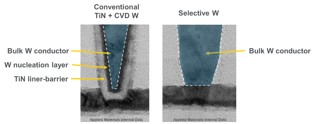
Figure 1: Applied’s Selective Tungsten (W) process technology eliminates the need for titanium nitride (TiN) liner-barriers so the entire contact via can be filled with conducting metal.
Another benefit of selective processing is that it allows designers to build chips in entirely new ways. It enables the creation and removal of new structures that were previously impossible to manufacture – even beneath the surface of the wafer and beyond the tool’s direct line-of-sight. By providing scalpel-like precision capability, selective processing promises to open new avenues in 3D fabrication by removing the constraints of conventional deposition and etch. For example, Applied’s selective etch process can be tuned to excavate and remove a specific material in a multi-layer stack to create novel 3D architectures such as Gate-All-Around which bring new levels of transistor performance (see Figure 2).
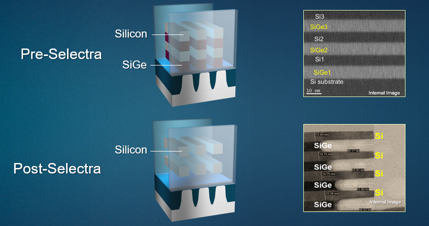
Figure 2: Images of a Gate-All-Around transistor showing how Applied’s Producer® Selectra® Etch system selectively removes silicon germanium (SiGe), which is beyond the tool’s direct line of sight, while leaving the desired silicon material intact.
Applied’s Selective Processing Portfolio
For nearly 20 years, Applied has been innovating selective materials solutions that eliminate roadblocks and drive the industry forward. These systems have enabled advancements in memory and logic designs. Today, the path to higher performance lies in supplementing continued 2D scaling with new 3D architectures enabled by materials engineering.
Applied’s breadth of process IP allows us to access a unique, cross-functional library of technologies to develop innovative integrated materials solutions. This is particularly important when it comes to selective processing methods, as the ability to clearly distinguish one material from another on the wafer is tied to atomic-level preparation of surfaces that can only be performed by bringing multiple clean and treatment technologies together in a pristine, high-vacuum environment.
Another capability enabled by Applied’s broad technology portfolio was described by my colleague Regina Freed in a previous blog, in which she explains how Applied is co-optimizing our selective deposition, selective etch, e-beam metrology and defect control technologies to eliminate misalignment between different device layers to solve edge placement errors (EPE) and improve scaling (see Figure 3).
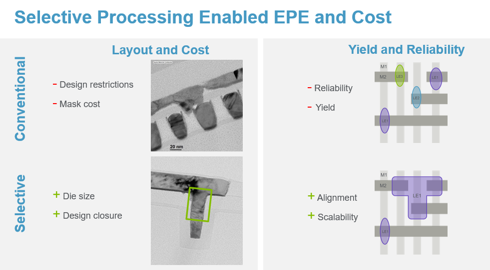
Figure 3: Fully selective, self-aligned processing can reduce resistance, increase yield and reduce mask count as compared to conventional processing.
At Applied, we are focused on leading the development of new techniques and IP for selectively adding, subtracting and shaping materials at an atomic scale. The addition of selective processing to the breadth of technologies within our portfolio provides another crucial building block to help our customers achieve their PPACt goals so that we can confidently march deeper into the AI Era.
Tags: AI Era, PPAC, selective processing, selective deposition, selective etch, gate-all-around, 3D, chip scaling
Zhebo Chen
Global Product Manager, Atomic Layer Deposition (ALD) & Metal Deposition Products (MDP)
Zhebo Chen is the head of product management for the ALD & MDP business units at Applied Materials, supporting a wide spectrum of deposition technologies including ALD, CVD & PVD. Zhebo holds a bachelor’s degree in Chemical Engineering from the University of Illinois at Urbana-Champaign and a Ph.D. in Chemical Engineering from Stanford University.

Adding Sustainability to the Definition of Fab Performance
To enable a more sustainable semiconductor industry, new fabs must be designed to maximize output while reducing energy consumption and emissions. In this blog post, I examine Applied Materials’ efforts to drive fab sustainability through the process equipment we develop for chipmakers. It all starts with an evolution in the mindset of how these systems are designed.

Innovations in eBeam Metrology Enable a New Playbook for Patterning Control
The patterning challenges of today’s most advanced logic and memory chips can be solved with a new playbook that takes the industry from optical target-based approximation to actual, on-device measurements; limited statistical sampling to massive, across-wafer sampling; and single-layer patterning control to integrative multi-layer control. Applied’s new PROVision® 3E system is designed to enable this new playbook.![]()

Breakthrough in Metrology Needed for Patterning Advanced Logic and Memory Chips
As the semiconductor industry increasingly moves from simple 2D chip designs to complex 3D designs based on multipatterning and EUV, patterning control has reached an inflection point. The optical overlay tools and techniques the semiconductor industry traditionally used to reduce errors are simply not precise enough for today’s leading-edge logic and memory chips.