Products & Technologies
Products & Services
Contact
Products & Services
Products & Technologies
Services
Resources
Contact
Posted
April 27, 2020

Stay updated on our content.
Materials-Enabled Patterning Helps Eliminate Trade-Offs in PPAC
by Regina Freed
Apr 27, 2020
In the golden days of the semiconductor industry, when Gordon Moore was still driving the roadmap for his companies, planar scaling delivered simultaneous improvements in power, performance and area/cost (PPAC). Over time, Dennard scaling stopped delivering power reductions, and materials engineering was added to the playbook so that power, performance and area/cost could continue to progress together. The high-k metal gate is a great example.
More recently, engineers have accepted trade-offs, with some designs optimized for power and performance, and others using aggressive 2D scaling to reduce area/cost. This divergent approach has led to a situation where the industry is capable of shrinking feature sizes to less than 8nm, but many designs are not adopting such small features in production, whether in foundry, logic or memory. While node nomenclatures imply shrinking device sizes, feature scaling is progressing more slowly than in the past. Moreover, we are seeing a dramatic slowdown in cost reduction (see Figure 1).
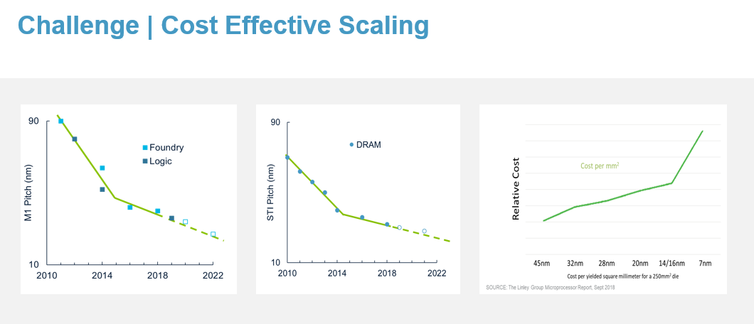
Figure 1: Complexity of chip designs is causing feature scaling to slow and costs to rise.
Why is scaling progressing more slowly than should be possible? Why is advanced silicon costing so much? The answer lies in the complexity of chip designs that now consist of multiple, dissimilar layers, each of which must be connected seamlessly.
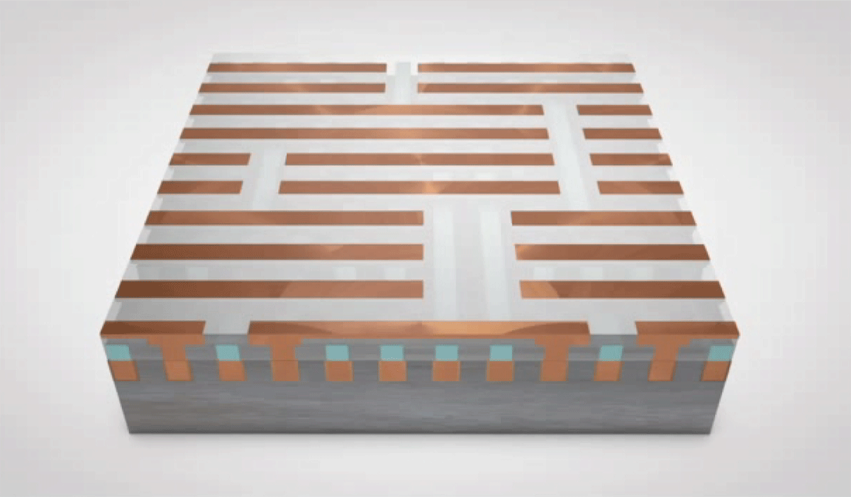
Take DRAM, for example. A DRAM device employs about seven critical patterning layers, none of which looks the same (see Figure 2). Aside from the different physical configurations of the shallow trench isolation (STI) layer, capacitors, bit lines and word lines, some layers have extremely high aspect ratios, which makes it increasingly difficult to align one layer with the next. Yet all of these different features need to be printed and aligned for the device to work properly. The process is complicated further by the fact that each of these very different layers must be made to shrink consistently. Otherwise, edge placement errors (EPE) can increase resistance, reduce performance, and introduce yield losses and device failures.
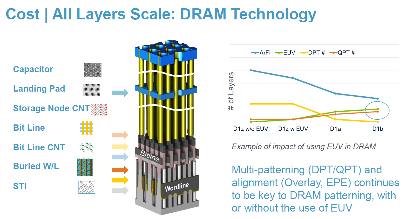
Figure 2: Dissimilar DRAM device layers create scaling and alignment challenges.
The roadmap faces roadblocks, and we need a “New Playbook” for improving chip performance, power and area-cost, along with time-to-market (PPACt). The New Playbook consists of:
- new computing architectures
- new on-chip devices and 3D structures
- new materials
- new ways to continue 2D scaling (the main topic of this blog)
- and heterogeneous design and advanced packaging.
From an equipment perspective, we need to do more than just introduce new films or improve unit process steps like etching. We need to think holistically and create suites of complementary techniques that can deliver improvements tailored to the needs of each device.
This evolution from unit processes to integrated materials solutions is also what’s needed to help customers remove process steps, reduce R&D cost and time, and accelerate time-to-market. What follows are three innovative techniques I unveiled earlier this year at the SPIE Advanced Lithography conference that show how a holistic approach to advanced patterning can benefit chipmakers across several vectors.
Square Spacers
Square spacers are used for self-aligned double patterning (SADP) and quadruple patterning (SAQP). Depositing and etching spacers is challenging, in part because the material used is relatively weak and subject to rounding at the top and bottom. This in turn leads to non-uniformity and pitch walking that introduces EPE in the form of lithography overlay errors and vertical misalignment—variation problems that become worse at smaller process nodes.
Chipmakers typically address variation by adding extra process steps, which increases cost and complexity. Additionally, while extra hard-mask etch and mandrel-etch steps can reduce some of the variability that comes from the first spacer etch, they degrade the resolution of the features that designers want to create at a specific pitch or critical dimension (CD). In other words, the very process steps that are intended to address EPE come with performance trade-offs that reduce the level of control over the design outcome.
A new technique developed by Applied Materials optimizes the spacer material to make it more friendly for the etch process, which results in better alignment (see Figure 3). Amorphous silicon is deposited with ALD-like precision using a CVD process. Then our Centris® Sym3™ etch system is used for patterning while our VeritySEM® system is employed for metrology. Our solution allows chipmakers to use conventional process steps and reduce the SAQP step count from 15 to 11 by eliminating unneeded deposition and etch steps while maintaining patterning fidelity. That, in turn, allows customers to scale much more cost-effectively.
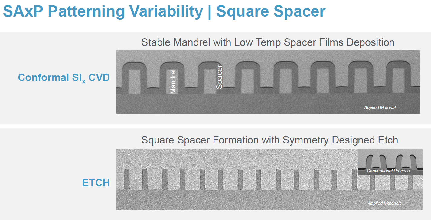
Figure 3: Applied’s unique spacer material results in much better uniformity and alignment compared to the conventional process.
Lateral Etch
Another unique capability developed by Applied is what we call lateral etch. Using conventional lithography and etch, there is a limit to how close designers can bring features together. In the horizontal direction it’s called the minimum pitch and in the vertical dimension it's called tip-to-tip. With EUV, the current minimum pitch is about 36nm, while tip-to-tip is about 40nm. If those distances are too large for the design, chipmakers are forced to invest in an extra patterning step—either an added cut or block mask or another EUV lithography-etch step. The only alternative to this is to keep the die larger, which increases area/cost.
Historically, etching has been performed top-down. Applied has developed an innovative lateral etch technique that gives designers a new degree of freedom by allowing etching at a 45-degree angle (see Figure 4). By controlling the direction of the etch, we can maintain the CD in one direction while we shrink the CD in the other. Likewise, we’ve demonstrated that we can independently reduce the CD and reduce tip-to-tip by about 20nm.
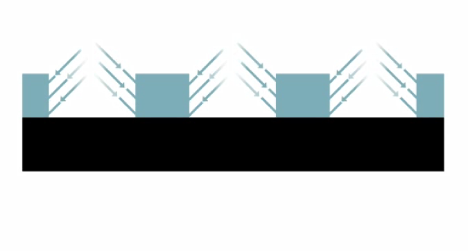
Figure 4: Applied’s innovative lateral etch capability can reduce EUV mask count by 50% or more.
Lateral etch can benefit many device applications by allowing designers to reduce process steps and bring features closer together to increase area density. By co-optimizing the process with our Producer® Precision™ CVD carbon and silicon hard masks, Sym3™ etch, and PROVision™ e-beam metrology and defect control for advanced patterning solutions, we give designers the opportunity to reduce EUV mask count by 50 percent or more.
Selective Processing
The third technique I unveiled at SPIE Advanced Lithography is a selective materials engineering process which addresses EPE by helping eliminate misalignment between different device layers to improve scaling. Unlike conventional deposition, selective processing works to eliminate EPE and thereby shrink design rules and mask count.
For selective deposition to be effective in reducing EPE, two key challenges must be overcome. First, the wafer surface must be kept exceptionally well-prepared and clean so that the deposition occurs only on the desired material and not others. Any defect on the wafer will compromise selectivity. The second challenge is effectively controlling the selectively deposited material which will tend to grow not just vertically but also horizontally. Because of these challenges, most selective deposition has been limited to very thin layers.
At Applied, we’ve developed a co-optimized selective processing solution using our Endura® platform for deposition, Producer® Selectra™ selective etch, and PROVision™ e-beam metrology and defect control. We’ve demonstrated this process as part of the via flow shown in Figure 5. We begin with a metal layer and then grow our selective material. Next, we perform gap fill and planarization. Then we perform traditional processing with a titanium-nitride (TiN) hard mask followed by the via lithography stack. We continue with lithography for the via and then move to the etch. When we etch in one direction, it's selective to the TiN that defines the trench. The other etch is selective using our newly developed material. This means that the via is perfectly etched as a rectangle defined where the two metal layers cross one another. This technique eliminates EPE by maximizing the size of the via, which also eliminates problems associated with interconnect scaling
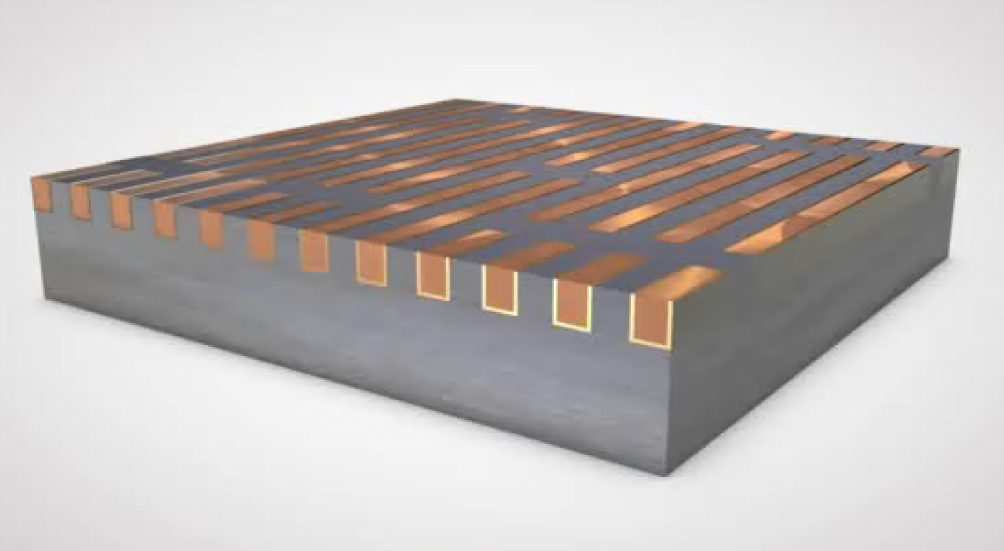
Figure 5: Video showing a via flow using a combination of Applied’s materials engineering capabilities to reduce mask count and improve EPE.
If a designer needs vias that are closer together than the minimum resolution of today’s lithography, they must perform multiple lithography-etch steps to define all the vias. With our new process, customers can now define one large via hole and create vias only on the crossover between the two metal layers. By doing so, we can perfectly align the bottom and top device layers, saving process steps and creating larger vias with better resistance (see Figure 6).
According to Dan Hutcheson, chairman and CEO of VLSIresearch, “What’s really new is that Applied has been able open up vias, thereby reducing EPE-induced yield loss while lowering cost compared to a conventional multi-patterned cut mask approach, and while shaving off 0.7nm out of the via. In addition to increasing yield, reducing EPE also increases revenue per-wafer due to improved reliability, performance and lower power drain on the chips.”
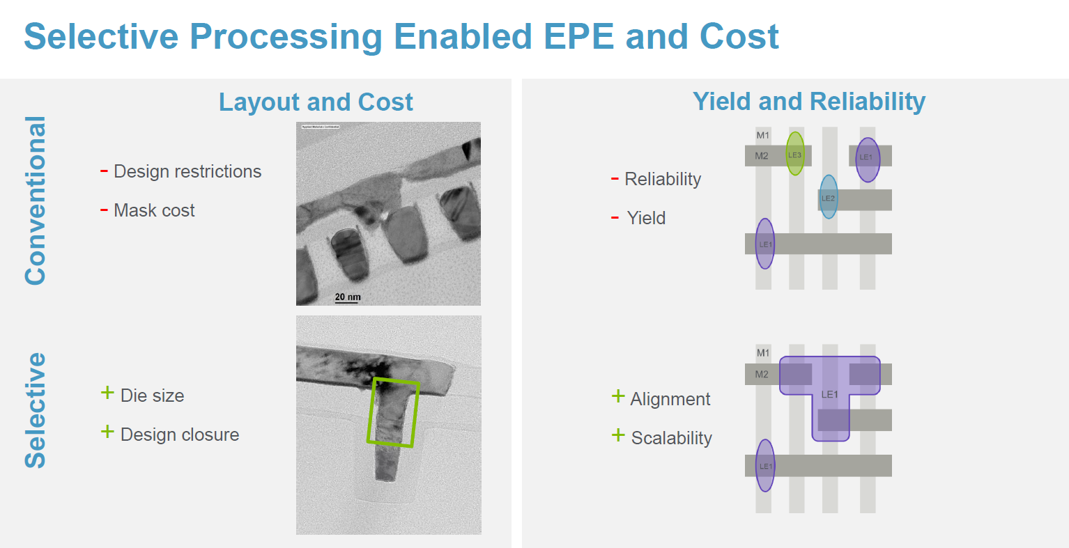
Figure 6: Fully selective, self-aligned processing can reduce resistance, increase yield and reduce mask count as compared to conventional processing.
The New Playbook gives us new tools to accelerate the industry’s roadmap, including by approaching scaling challenges holistically to address all aspects of PPACt simultaneously. By co-optimizing Applied’s broad technology suite we can deliver new materials that enable new ways to shrink and allow cost-effective scaling to continue without design compromises. Welcome to the materials-enabled patterning era!
Tags: materials engineering, Patterning, PPAC, PPACt, New Playbook, DRAM, SPIE Advanced Lithography, EPE, logic
Regina Freed
Vice President, AIx™ Solutions

Regina Freed has more than 20 years of experience in the semiconductor industry, managing semiconductor process and equipment development for both logic and memory processes, including co-optimization between deposition and etch, lithography, metrology, and defect inspection. At Applied Materials, Regina leads our AIx™ program that enables us and our customers to accelerate development and ramp through Actionable Insights as well as control our processes to deliver improved process windows, enabling customers to scale faster and at lower cost, while optimizing device performance.

Adding Sustainability to the Definition of Fab Performance
To enable a more sustainable semiconductor industry, new fabs must be designed to maximize output while reducing energy consumption and emissions. In this blog post, I examine Applied Materials’ efforts to drive fab sustainability through the process equipment we develop for chipmakers. It all starts with an evolution in the mindset of how these systems are designed.

Innovations in eBeam Metrology Enable a New Playbook for Patterning Control
The patterning challenges of today’s most advanced logic and memory chips can be solved with a new playbook that takes the industry from optical target-based approximation to actual, on-device measurements; limited statistical sampling to massive, across-wafer sampling; and single-layer patterning control to integrative multi-layer control. Applied’s new PROVision® 3E system is designed to enable this new playbook.

Breakthrough in Metrology Needed for Patterning Advanced Logic and Memory Chips
As the semiconductor industry increasingly moves from simple 2D chip designs to complex 3D designs based on multipatterning and EUV, patterning control has reached an inflection point. The optical overlay tools and techniques the semiconductor industry traditionally used to reduce errors are simply not precise enough for today’s leading-edge logic and memory chips.