Products & Technologies
Products & Services
Contact
Products & Services
Products & Technologies
Services
Resources
Contact
Posted
July 20, 2020

Stay updated on our content.
Introducing a Breakthrough in 2D Scaling
by Zhebo Chen
Jul 20, 2020
Applied Materials has introduced a breakthrough in materials engineering: selective tungsten deposition.
The shrinking of feature sizes with EUV lithography is exacerbating contact resistance in the crucial, first level of wiring that connects the transistor to the rest of the wiring in the chip. This has become the fundamental challenge to continued 2D scaling: as the interconnect wiring gets thinner, resistance increases. The industry needs new materials and materials engineering techniques that offer new ways to scale.
As I explained in my previous blogs, transistor contacts are formed in ever-smaller vias where a titanium nitride liner-barrier and tungsten nucleation layers are formed and then filled with tungsten contact metal. The liner-barrier provides adherence to the via sidewall while the nucleation layer permits bulk tungsten to grow. In my last blog, I used the analogy of painting a wooden fence: a primer layer and thin, first coat is applied to ensure the thicker, second coat applies smoothly and adheres without peeling (see Figure 1).
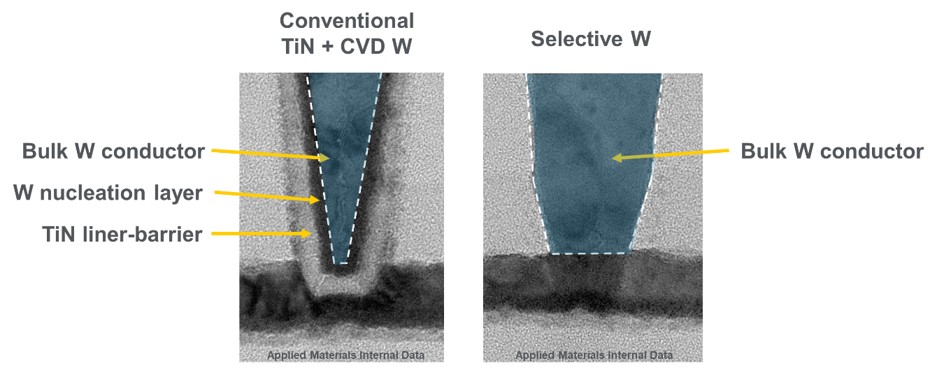
Figure 1: Applied’s Selective Tungsten (W) process technology eliminates the need for titanium nitride (TiN) liner-barriers so the entire contact via can be filled with conducting metal.
This decades-old approach has become a critical challenge to continued 2D scaling because the liner-barrier does not scale, leaving less space for tungsten conductor metal with each successive node. The thinner the tungsten conductor, the higher the resistance.
At the 7nm foundry node, the contact via is about 20nm in diameter. The liner-barrier and nucleation layers occupy approximately 75 percent of the via’s volume, leaving only around 25 percent for tungsten. The increasing resistance offsets the performance potential of having a greater number of smaller and more advanced transistors, and the issue only becomes worse as the vias continue to shrink at the 5nm node and beyond.
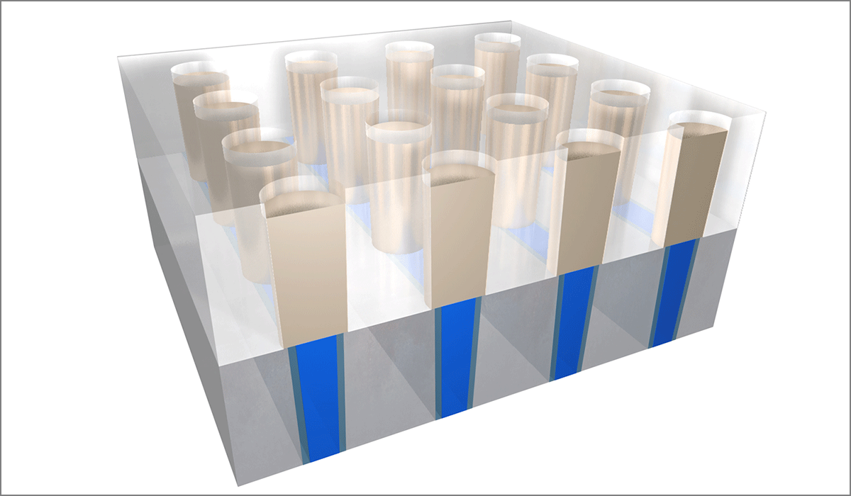
To solve this bottleneck to continued 2D scaling and PPAC, Applied has developed a breakthrough called selective tungsten deposition that gives chipmakers an entirely new way to build the transistor contacts. The new process enables chipmakers to eliminate the liner-barrier and nucleation layers—and selectively fill the entire via with low-resistance tungsten. Applied’s new selective process is like 3D printing at the atomic scale (see Figure 2).
Conventional Approach Metal Volume Reduced by Liner-Barrier and Nucleation Layer
Selective Process Metal Volume Maximized Using Bottom-Up Growth
Figure 2: The Selective Tungsten process grows bottom-up from the underlying metal to achieve void-free and seam-free gap fill, without the cladding required by conventional tungsten CVD.
The selective deposition is enabled by the new Endura® Volta™ Selective Tungsten CVD system. It’s an Integrated Materials Solution in which the wafer travels through multiple high-vacuum chambers that are many times cleaner than the cleanroom itself. Atomic-level surface treatments are applied to the wafer to remove all atomic-level impurities, and tungsten atoms are made to selectively adhere to the bottom of the via only and then fill the via from the bottom up with no delamination, voids or seams which could negatively impact power consumption, performance and yield (see Figure 3).
Figure 3: The Integrated Materials Solution on the Endura® platform allows the wafer to undergo multiple processes without ever breaking vacuum. This pristine process environment is critical to achieving selective tungsten deposition.
The result is a contact with a larger volume of tungsten and a clean metal-to-metal interface to the underlying metal, resulting in a significant reduction in contact resistance. Removing the resistance bottleneck makes it is easier for electrons to flow, which translates to improved device power and performance.
The ability to deploy this high-precision process in high-volume manufacturing is a huge feat of materials engineering. Consider that each contact is just 1/2,000th the width of a human hair and that there are hundreds of billions of contacts on every die, which translates to more than 100 kilometers of tungsten contact wiring on every wafer.
The Integrated Materials Solution is key to achieving deposition precision and reliability in high volume production. The technology solves a tungsten deposition challenge that has eluded the industry for over 30 years.
The new Endura system for selective tungsten deposition is being used by multiple leading customers worldwide and is on the roadmap to enable several generations of continued 2D scaling.
Applied Materials believes selective processing—both deposition and removal—will be key enablers of continued 2D scaling and of 3D architectures that add a new dimension to bit and transistor density scaling.
Stay tuned for my next and final blog in this series which will discuss how the new Endura system for selective tungsten extends Applied’s selective processing portfolio—a collection of innovative technologies that allow chipmakers to create, shape and modify materials in entirely new ways to enable continued advances in PPAC.
Tags: AI Era, PPAC, EUV, lithography, transistor scaling, contact via, contact resistance, interconnect
Zhebo Chen
Global Product Manager, Atomic Layer Deposition (ALD) & Metal Deposition Products (MDP)

Zhebo Chen is the head of product management for the ALD & MDP business units at Applied Materials, supporting a wide spectrum of deposition technologies including ALD, CVD & PVD. Zhebo holds a bachelor’s degree in Chemical Engineering from the University of Illinois at Urbana-Champaign and a Ph.D. in Chemical Engineering from Stanford University.

Adding Sustainability to the Definition of Fab Performance
To enable a more sustainable semiconductor industry, new fabs must be designed to maximize output while reducing energy consumption and emissions. In this blog post, I examine Applied Materials’ efforts to drive fab sustainability through the process equipment we develop for chipmakers. It all starts with an evolution in the mindset of how these systems are designed.

Innovations in eBeam Metrology Enable a New Playbook for Patterning Control
The patterning challenges of today’s most advanced logic and memory chips can be solved with a new playbook that takes the industry from optical target-based approximation to actual, on-device measurements; limited statistical sampling to massive, across-wafer sampling; and single-layer patterning control to integrative multi-layer control. Applied’s new PROVision® 3E system is designed to enable this new playbook.

Breakthrough in Metrology Needed for Patterning Advanced Logic and Memory Chips
As the semiconductor industry increasingly moves from simple 2D chip designs to complex 3D designs based on multipatterning and EUV, patterning control has reached an inflection point. The optical overlay tools and techniques the semiconductor industry traditionally used to reduce errors are simply not precise enough for today’s leading-edge logic and memory chips.