Products & Technologies
Products & Services
Contact
Products & Services
Products & Technologies
Services
Resources
Contact
Posted
July 16, 2020

Stay updated on our content.
Solving Transistor Contact Resistance Requires Materials Engineering Innovations

by Zhebo Chen
Jul 16, 2020
In my previous blog, I described how increasing contact resistance is becoming a major bottleneck to transistor power and performance.
Now I will explain why contact resistance has become more challenging to the foundry-logic roadmap, reaching a point where an entirely new approach to building transistor contacts is needed to scale to the 5nm node and beyond.
Previously, I explained how the cladding layers in tungsten (W) transistor contacts are becoming a major cause of contact resistance. The cladding is in the form of a titanium nitride (TiN) liner-barrier and a W nucleation layer. These layers serve a critical function of ensuring that the contact adheres well to surfaces and grows evenly, without defects—but they do a very poor job of conducting electrons.
To make an analogy, think about painting a wooden fence: you apply a coat of primer before applying a thin, first coat of paint and then a thick, final coat. Similarly, without the TiN barrier, the bulk W adheres poorly to the surfaces and simply flakes off. Without the W nucleation layer, the bulk W doesn’t grow.
Unfortunately, these “preparation layers” have become increasingly problematic because they do not scale. The result is that a higher percentage of the available volume goes to the liner-barrier while a dwindling percent goes to the W conductor. With each foundry-logic node, contact resistance increases, starving the finely engineered transistor and chip and preventing them from achieving their power and performance potential.
Another challenge to the traditional W fill process is that a seam forms, further increasing resistance and potentially impacting yield in high-volume production (see Figure 1).
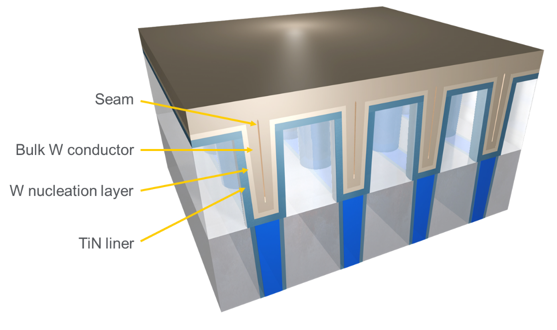
Figure 1: Conventional CVD tungsten deposition.
Over the years, the industry has focused on lowering contact resistance primarily by reducing the volume of the liner-barrier layers and introducing new contact materials. For example, in 2016, Applied introduced a new film that could replace the TiN liner-barrier and W nucleation layers with one tungsten-carbon film, providing more volume for bulk W. We also offered a solution designed to suppress seam formation during bulk W fill. Two years later, Applied introduced a cobalt alternative to bulk W which further thinned the TiN liner and could be grown without a nucleation layer. While more effective, these solutions still relied on “primer” layers to reliably grow the metal conductors. However, as contact vias scale further with the introduction of EUV, the industry needs a bigger breakthrough.
The optimal solution would be to remove the cladding layers altogether and achieve a perfect bottom-up fill with no voids or seams. This has not been achievable with conventional chemical vapor deposition because it deposits material across the entire wafer surface, with poor control for sidewall adhesion and growth. The cladding layers are needed to ensure smooth growth and a complete gap fill.
In my next blog, I’ll describe a unique, Integrated Materials Solution which provides a materials engineering breakthrough aimed at solving the contact resistance bottleneck and enabling 2D scaling to continue well into the future.
Tags: AI Era, PPAC, EUV, lithography, transistor scaling, contact via, contact resistance, interconnect
Zhebo Chen
Global Product Manager, Atomic Layer Deposition (ALD) & Metal Deposition Products (MDP)

Zhebo Chen is the head of product management for the ALD & MDP business units at Applied Materials, supporting a wide spectrum of deposition technologies including ALD, CVD & PVD. Zhebo holds a bachelor’s degree in Chemical Engineering from the University of Illinois at Urbana-Champaign and a Ph.D. in Chemical Engineering from Stanford University.

Adding Sustainability to the Definition of Fab Performance
To enable a more sustainable semiconductor industry, new fabs must be designed to maximize output while reducing energy consumption and emissions. In this blog post, I examine Applied Materials’ efforts to drive fab sustainability through the process equipment we develop for chipmakers. It all starts with an evolution in the mindset of how these systems are designed.

Innovations in eBeam Metrology Enable a New Playbook for Patterning Control
The patterning challenges of today’s most advanced logic and memory chips can be solved with a new playbook that takes the industry from optical target-based approximation to actual, on-device measurements; limited statistical sampling to massive, across-wafer sampling; and single-layer patterning control to integrative multi-layer control. Applied’s new PROVision® 3E system is designed to enable this new playbook.

Breakthrough in Metrology Needed for Patterning Advanced Logic and Memory Chips
As the semiconductor industry increasingly moves from simple 2D chip designs to complex 3D designs based on multipatterning and EUV, patterning control has reached an inflection point. The optical overlay tools and techniques the semiconductor industry traditionally used to reduce errors are simply not precise enough for today’s leading-edge logic and memory chips.