Products & Technologies
Products & Services
Contact
Products & Services
Products & Technologies
Services
Resources
Contact
Posted
July 08, 2020

Stay updated on our content.
Transistor Scaling Gated by Contact Resistance

by Zhebo Chen
Jul 08, 2020
At Applied Materials, we are working closely with our customers to help them solve the semiconductor design and manufacturing challenges of the AI Era.
For decades, the industry relied on classic 2D scaling to drive simultaneous improvements in power, performance and area/cost (PPAC), but that playbook has become more challenging.
The advent of EUV lithography has helped overcome some of the 2D scaling challenges, but at the same time it has brought to light other problems that are becoming more critical as transistor feature sizes shrink. In this blog, the first in a series, I will explore the issue of contact resistance and explain why it is becoming a growing impediment to transistor power and performance scaling—and why a breakthrough in materials engineering is needed.
The contacts are the first and one of the smallest levels of wiring that connects the transistor to the rest of the wiring in the chip. The contacts help drive electrons across the channel once the gate activates the transistor into its “on” state (see Figure 1).
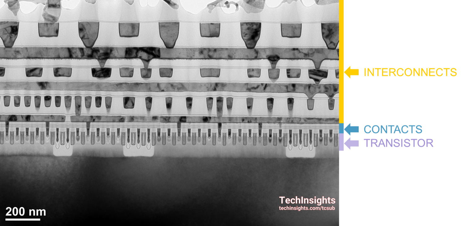
Figure 1: Close-up of transistors, contacts and interconnects.
For many years, transistor contacts have been formed by creating vias within a dielectric layer, cladding the vias with liner-barriers and nucleation layers and filling the remaining portion of the via with tungsten (W), the contact metal of choice due to its low resistivity.
The liner-barrier is typically composed of titanium nitride (TiN) which is good at adhering to the sidewall of the via and preventing defects like delamination and voids. Because tungsten doesn’t naturally grow on TiN, a W nucleation layer is deposited before the W bulk fill. The TiN liner and W nucleation layer are like a mold that defines the space for the W contact (see Figure 2). Although this mold takes up a large percentage of the via’s space, it does little to conduct electrons because its resistance is much higher than that of bulk W.
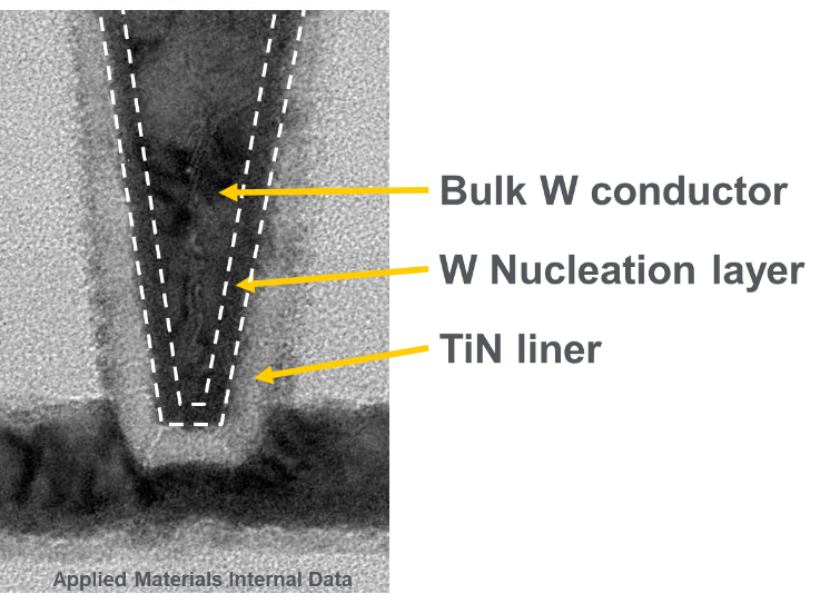
Figure 2: Conventional tungsten deposition with liner and nucleation layer.
With the advent of EUV lithography, the contact vias can continue to scale. But contact power and performance are hitting the wall: the “mold” is now taking up more volume than the contact metal, and contact resistance is growing (see Figure 3). Without a breakthrough in contact metal deposition, there is no benefit to shrinking: the transistor is like a Formula 1 race car stuck in rush hour traffic.
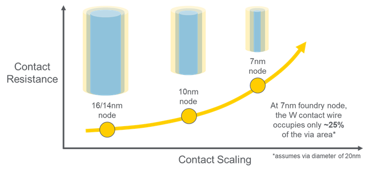
Figure 3: As the diameter of the contact via shrinks, resistance increases and performance slows.
In my next blog, I’ll describe some of the techniques Applied Materials has developed to relieve the contact resistance bottleneck—and why more work is needed to enable new ways to shrink.
Tags: AI Era, PPAC, EUV, lithography, transistor scaling, contact via, contact resistance, interconnect
Zhebo Chen
Global Product Manager, Atomic Layer Deposition (ALD) & Metal Deposition Products (MDP)

Zhebo Chen is the head of product management for the ALD & MDP business units at Applied Materials, supporting a wide spectrum of deposition technologies including ALD, CVD & PVD. Zhebo holds a bachelor’s degree in Chemical Engineering from the University of Illinois at Urbana-Champaign and a Ph.D. in Chemical Engineering from Stanford University.

Adding Sustainability to the Definition of Fab Performance
To enable a more sustainable semiconductor industry, new fabs must be designed to maximize output while reducing energy consumption and emissions. In this blog post, I examine Applied Materials’ efforts to drive fab sustainability through the process equipment we develop for chipmakers. It all starts with an evolution in the mindset of how these systems are designed.

Innovations in eBeam Metrology Enable a New Playbook for Patterning Control
The patterning challenges of today’s most advanced logic and memory chips can be solved with a new playbook that takes the industry from optical target-based approximation to actual, on-device measurements; limited statistical sampling to massive, across-wafer sampling; and single-layer patterning control to integrative multi-layer control. Applied’s new PROVision® 3E system is designed to enable this new playbook.

Breakthrough in Metrology Needed for Patterning Advanced Logic and Memory Chips
As the semiconductor industry increasingly moves from simple 2D chip designs to complex 3D designs based on multipatterning and EUV, patterning control has reached an inflection point. The optical overlay tools and techniques the semiconductor industry traditionally used to reduce errors are simply not precise enough for today’s leading-edge logic and memory chips.