Products & Technologies
Products & Services
Contact
Products & Services
Products & Technologies
Services
Resources
Contact
Posted
March 10, 2022

Stay updated on our content.
WFE Intensity Step-up: 3D NAND Case Study

Mar 10, 2022
After declining significantly from 2000 to 2015, we estimate that the NAND wafer fab equipment (WFE) intensity trendline took a 10-point step higher—from around 15% to around 25%—driven by the 2D to 3D NAND inflection. NAND WFE intensity has remained sustainably higher ever since. Let’s examine the factors that led to this increase.
3D NAND Case Study
Our analysis suggests that from 2000 to 2015, NAND WFE intensity decreased by nearly 30 points, from around 50% to around 20% (represented by the dotted line in Chart 1). While NAND revenues increased, annualized NAND bit growth gradually declined over this period owing to the deceleration of classic 2D scaling, which is consistent with our Battle of Exponentials framework. Toward the end of this period, NAND makers began a transition from 2D to 3D architectures. We estimate that the industry’s transition to 3D (represented by the shaded area in Chart 1) progressed from less than 10% of NAND capacity in 2015 to greater than 80% in 2021 as the new architecture permeated most NAND applications.
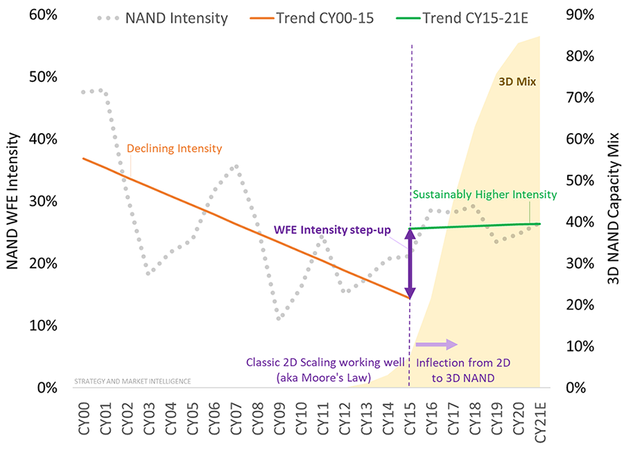
Chart 1: Inflection in NAND WFE Intensity. Source: Applied Materials - Strategy & Market Intelligence.
2D to 3D Transition = Higher WFE Intensity
As I wrote in my previous blog post, WFE intensity is driven by capacity and complexity. The latter often triggers the former. 3D NAND introduces an increasing number of new steps (complexity) compared to 2D NAND. Accordingly, NAND makers built new (a.k.a. greenfield) fabs suited to the new technology to demonstrate viability prior to converting 2D fabs to 3D, which they did later.
From Exponential Moore’s Law Scaling to Decelerating 3D Scaling
3D NAND scaling is different in another important way. While successive generations of 2D NAND scaling generated exponential bit growth, each increase in a defined number of 3D NAND layers results in progressively slower bit growth. Simply put, while the transition from 32L to 64L TLC devices produced 100% bit growth, the 64L to 96L transition produced only 50% bit growth, and the 96L to 128L transition produced only 33% bit growth. As percent bit growth moderates, manufacturers either need to accelerate the number of layers and steps, or they need to add wafer capacity. Either way, NAND WFE is sustainably higher.
Chart 2 illustrates that in the 2015 timeframe, the greenfield capacity cost for a given number of 3D NAND wafer starts was about 1.5X the cost of 2D NAND, and the delta widened to 2.2X by 2021.
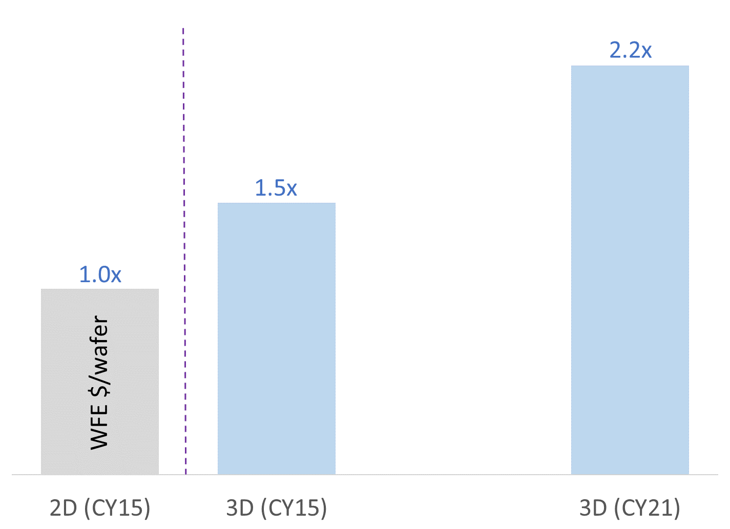
Chart 2: 2D vs. 3D NAND WFE $/wafer*. Source: Applied Materials - Strategy & Market Intelligence.
In addition to helping us think about NAND WFE intensity, we believe our 3D NAND case study may be instructive as we anticipate the potential impact of future 3D architecture transitions expected in DRAM and Foundry/Logic.
*Average WFE $/wafer across comparable technologies from multiple NAND makers.
Tags: NAND, WFE, WFE Intensity, Exponential, Moore's Law
Sundeep Bajikar
Corporate Vice President, Corporate Strategy and Marketing
Sundeep is Head of Corporate Strategy and Marketing (CSM) and guides the executive leadership team in the development of the company's growth thesis, strategic priorities, key initiatives and investor communications. He is also responsible for developing Applied’s marketing capabilities and community. Sundeep’s work served as the foundation for Applied’s strategies related to AI, ICAPS, Heterogenous Integration and Net Zero.
He joined Applied in 2017 after spending ten years as a Senior Equity Research Analyst covering global technology stocks, including Apple and Samsung Electronics, for Morgan Stanley and Jefferies. Previously he worked for a decade as a researcher, ASIC design engineer, system architect and strategic planning manager at Intel Corporation.
Sundeep holds an MBA in finance from The Wharton School and M.S. degrees in electrical engineering and mechanical engineering from the University of Minnesota. He holds 13 U.S. and international patents with more than 30 additional patents pending. Sundeep is also author of a book titled, “Equity Research for the Technology Investor – Value Investing in Technology Stocks.” He was an Institutional Investor Rising Star.

A New Normal for Semiconductor Growth?
In this blog I illustrate how the semiconductor revenue CAGR has increased in recent years and explain why growth could continue at this higher rate for the foreseeable future.

Battle of Exponentials — A Different Way to Think About Accelerating Semiconductor Growth
Semiconductor growth has accelerated to higher levels that may represent a new normal as suggested by our “battle of exponentials” framework.
Expanding the Ecosystem for Hybrid Bonding Technology
Applied Materials recently entered a new phase of our R&D collaboration with A*STAR’s Institute of Microelectronics to accelerate materials, equipment and process technology solutions for hybrid bonding and other emerging, 3D chip integration technologies.