Products & Technologies
Products & Services
Contact
Products & Services
Products & Technologies
Services
Resources
Contact
Posted
January 14, 2022

Stay updated on our content.
Battle of Exponentials — A Different Way to Think About Accelerating Semiconductor Growth

Jan 14, 2022
Recent increases in semiconductor growth may be explained by an ongoing battle between two exponentials: 1) the upward-sloping growth of data generation, which drives semiconductor unit demand, and 2) the downward sloping reduction in transistor costs driven by classic 2D Moore’s Law scaling, which drives ASP reductions.
Data have continued to grow exponentially, stimulating unit demand. But in recent years, the pace of transistor cost declines has moderated. This helps explain why semiconductor revenue growth has accelerated, as shown in the chart below.
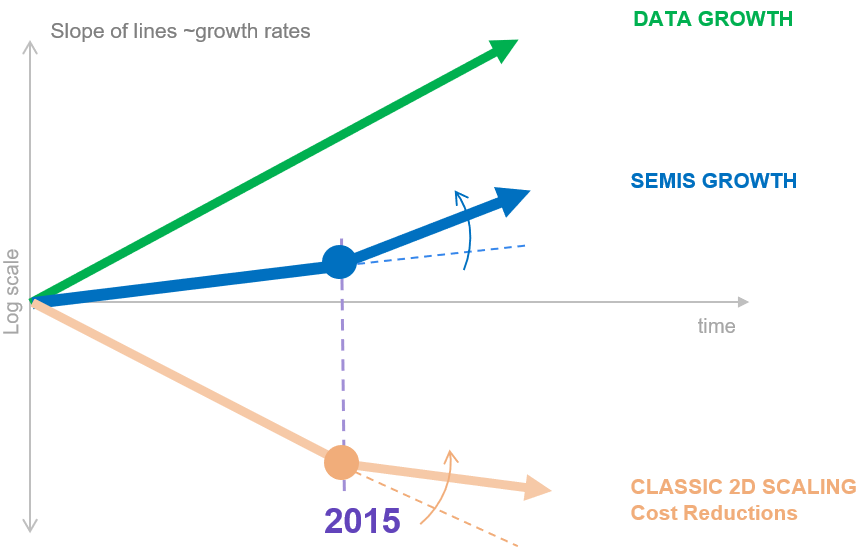
Chart 1: Battle of Exponentials. Source: Applied Materials—Strategy & Market Intelligence
A third exponential is network effects (more about these in a moment), which are also compounding and putting upward pressure on semiconductor demand.
For chipmakers, this battle of exponentials bodes well for revenue growth, profitability and the ability to invest for the future. It can also serve as a catalyst for new methods beyond classic Moore’s Law scaling that can deliver the cost reductions in computation needed to make it affordable to extract value as data multiply.
Data Exponential Amplified by AI
We estimate machine-generated data first exceeded human-generated data in 2018. Our proprietary data model suggests that by around 2025, machines will generate 99 percent of data created, fueled by a confluence of emerging applications including AI, the Internet of Things (IoT), blockchain, the metaverse and Web 3.0. Arguably still in their infancy, these applications create new, virtuous cycles, with increasing data generation requiring commensurate increases in data processing.
Just as machines are generating more data than humans, they are also making more decisions. AI turns data into commercial insights, and it is being deployed at scale, including for applications that were previously considered too complex or specialized to be automated.
Rise of Network Effect Technologies
Blockchain, social media and gaming exemplify applications that increase in value in accordance with Metcalfe’s Law, i.e., proportionate to the square of the number of participants. Human brains are wired to think in linear terms and often struggle to comprehend exponential effects in advance of them playing out. The premium valuations now accorded to social media companies, gaming companies and the Bitcoin network are recognition that the financial markets are catching on to the power and value of network effects.
Beyond Classic 2D Scaling
When Moore’s Law was functioning like clockwork (through around 20151), each new generation of advanced fab technology simultaneously enabled a doubling of transistors per chip, greater functionality, higher performance and lower cost. Affordable transistors fueled growth for the electronics industry, and investments and profits were concentrated in technologies aimed at further classic 2D scaling. Specialty nodes for markets Applied Materials calls ICAPS (IoT, Communications, Automotive, Power and Sensors) did not receive a lot of attention or investment dollars. However, over the past 18 months of IC shortages, the world has become acutely aware of the importance of a wide range of semiconductors that rely far less on shrinking to deliver value. The industry is changing, with demand and investments for semiconductor manufacturing becoming more evenly distributed between leading nodes and ICAPS nodes.
In my next blog post, I’ll share additional data about semiconductor growth—and explain additional ways to interpret the growth using the “battle of exponentials” framework.
1 Computer Architecture: A Quantitative Approach, Sixth Edition, John Hennessy and David Patterson, December 2017
Tags: Moore's Law, Network Effect, Exponential, AI, artificial intelligence, Big Data, iot, internet of things, Metaverse, Blockchain, ICAPS
Sundeep Bajikar
Corporate Vice President, Corporate Strategy and Marketing

Sundeep is Head of Corporate Strategy and Marketing (CSM) and guides the executive leadership team in the development of the company's growth thesis, strategic priorities, key initiatives and investor communications. He is also responsible for developing Applied’s marketing capabilities and community. Sundeep’s work served as the foundation for Applied’s strategies related to AI, ICAPS, Heterogenous Integration and Net Zero.
He joined Applied in 2017 after spending ten years as a Senior Equity Research Analyst covering global technology stocks, including Apple and Samsung Electronics, for Morgan Stanley and Jefferies. Previously he worked for a decade as a researcher, ASIC design engineer, system architect and strategic planning manager at Intel Corporation.
Sundeep holds an MBA in finance from The Wharton School and M.S. degrees in electrical engineering and mechanical engineering from the University of Minnesota. He holds 13 U.S. and international patents with more than 30 additional patents pending. Sundeep is also author of a book titled, “Equity Research for the Technology Investor – Value Investing in Technology Stocks.” He was an Institutional Investor Rising Star.

Expanding the Ecosystem for Hybrid Bonding Technology
Applied Materials recently entered a new phase of our R&D collaboration with A*STAR’s Institute of Microelectronics to accelerate materials, equipment and process technology solutions for hybrid bonding and other emerging, 3D chip integration technologies.

Adding Sustainability to the Definition of Fab Performance
To enable a more sustainable semiconductor industry, new fabs must be designed to maximize output while reducing energy consumption and emissions. In this blog post, I examine Applied Materials’ efforts to drive fab sustainability through the process equipment we develop for chipmakers. It all starts with an evolution in the mindset of how these systems are designed.

Innovations in eBeam Metrology Enable a New Playbook for Patterning Control
The patterning challenges of today’s most advanced logic and memory chips can be solved with a new playbook that takes the industry from optical target-based approximation to actual, on-device measurements; limited statistical sampling to massive, across-wafer sampling; and single-layer patterning control to integrative multi-layer control. Applied’s new PROVision® 3E system is designed to enable this new playbook.