Products & Technologies
Products & Services
Contact
Products & Services
Products & Technologies
Services
Resources
Contact
Posted
January 27, 2022

Stay updated on our content.
How to Think About Rising WFE Intensity
Jan 28, 2022
Defining WFE Intensity
Wafer fab equipment (WFE) is the market for specialized machines needed to fabricate semiconductor chips. WFE intensity refers to the proportion of semiconductor revenue invested in WFE to enable continued growth.
WFE intensity (%) = WFE ($) ÷ Semiconductor Revenues ($) * 100
WFE intensity increases primarily for two reasons: capacity and complexity. 1) Semiconductor fabs need more equipment to increase capacity so they can process more wafers and meet increasing demand for semiconductors. Conventional thinking is that capacity is the primary driver of WFE intensity. 2) Manufacturers add more wafer processing steps to produce more complex circuitry at higher levels of integration, thereby enabling more capable chips at a lower cost per function.
The Battle of Exponentials and WFE Intensity
Our Battle of Exponentials framework highlights an inflection in the semiconductor industry in the 2015 timeframe, including an inflection in WFE intensity. Between 2000 and 2015, WFE intensity was downward sloping, but it has been climbing since (see Chart 1). Factors contributing to the downslope included 1) the transition from 200mm to more productive 300mm wafer sizes in advanced logic and memory, 2) a consistent cadence of classic Moore’s Law 2D shrinks, and 3) consolidation of semiconductor manufacturing and architectures.
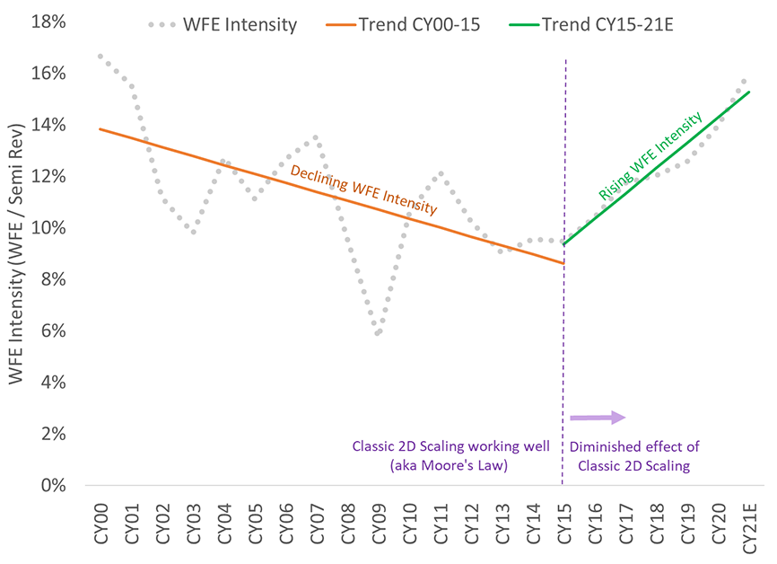
Chart 1: Inflection in WFE Intensity. Source: Applied Materials - Strategy & Market Intelligence.
Wafer Size Limited to 300mm = Higher WFE Intensity
A larger wafer can fit more chips, and the transition from 200mm to 300mm enabled chipmakers to produce 2.25X the number of like-sized chips with each wafer. Accordingly, as more of the semiconductor industry transitioned to 300mm wafers, WFE intensity declined. The industry has fully suspended efforts to develop even larger 450mm wafers, so we don’t expect wafer size transitions to constrain WFE growth in the foreseeable future.
Classic 2D Scaling Not Working Well = Higher WFE Intensity
If wafers aren’t getting bigger, and you can’t get more chips per wafer by shrinking the size of each chip through classic 2D scaling, then you simply need to add more wafers to make more chips. In fact, average die sizes of many kinds of chips is increasing. As a result, we are seeing public announcements of the largest number of new, greenfield wafer fab plans in years—particularly in foundry/logic, in both leading-edge and ICAPS nodes.
Diversification of Computing Architectures = Higher WFE Intensity
When Moore’s Law worked well, computing applications concentrated on one prevailing architecture (x86). Exponential increases in transistor budgets and increasing clock speeds gave system designers and programmers the performance they needed to keep up with most workload requirements, which at the time focused on PCs and servers. As computing applications diversified toward mobility and 3D visual computing—and later to more parallel workloads used to accelerate deep learning (AI) and proof-of-work blockchain (e.g. Bitcoin)—architectures proliferated. Today, high-performance computing (HPC) workloads are a leading driver of WFE investments.
In my next blog post I’ll demonstrate that the combination of higher semiconductor growth and higher WFE intensity is driving a secular step-up in WFE growth.
Tags: WFE, WFE Intensity, Moore's Law, Exponential, AI, deep ultraviolet, High-performance Computing, HPC, Blockchain, ICAPS, Foundry, logic
Sundeep Bajikar
Corporate Vice President, Corporate Strategy and Marketing
Sundeep is Head of Corporate Strategy and Marketing (CSM) and guides the executive leadership team in the development of the company's growth thesis, strategic priorities, key initiatives and investor communications. He is also responsible for developing Applied’s marketing capabilities and community. Sundeep’s work served as the foundation for Applied’s strategies related to AI, ICAPS, Heterogenous Integration and Net Zero.
He joined Applied in 2017 after spending ten years as a Senior Equity Research Analyst covering global technology stocks, including Apple and Samsung Electronics, for Morgan Stanley and Jefferies. Previously he worked for a decade as a researcher, ASIC design engineer, system architect and strategic planning manager at Intel Corporation.
Sundeep holds an MBA in finance from The Wharton School and M.S. degrees in electrical engineering and mechanical engineering from the University of Minnesota. He holds 13 U.S. and international patents with more than 30 additional patents pending. Sundeep is also author of a book titled, “Equity Research for the Technology Investor – Value Investing in Technology Stocks.” He was an Institutional Investor Rising Star.

A New Normal for Semiconductor Growth?
In this blog I illustrate how the semiconductor revenue CAGR has increased in recent years and explain why growth could continue at this higher rate for the foreseeable future.

Battle of Exponentials — A Different Way to Think About Accelerating Semiconductor Growth
Semiconductor growth has accelerated to higher levels that may represent a new normal as suggested by our “battle of exponentials” framework.
Expanding the Ecosystem for Hybrid Bonding Technology
Applied Materials recently entered a new phase of our R&D collaboration with A*STAR’s Institute of Microelectronics to accelerate materials, equipment and process technology solutions for hybrid bonding and other emerging, 3D chip integration technologies.