Products & Technologies
Back to Menu
Products & Technologies
Services
Resources
Posted
June 16, 2021

Stay updated on our content.
Materials Engineering is Key to Enabling Continued Logic Scaling
Jun 16, 2021
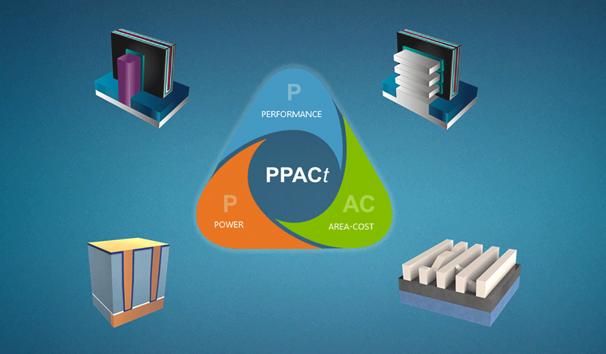
Applied Materials hosted an online Logic Master Class today where we showcased several materials engineering solutions that enable advanced logic scaling with continued improvements in power, performance, area, cost and time to market (PPACt™).
As my colleagues outlined in recent blogs, multiple challenges impede power and performance improvements when scaling transistors and interconnects to the 3nm node and beyond. There are also pattern variability issues which require new materials engineering solutions. In this blog I will highlight how Applied is helping enable our customers’ PPACt roadmaps for advanced logic with innovations based on co-optimization of process steps and Integrated Materials Solutions (IMS™). We are also helping the industry implement a scaling technique called Design Technology Co-Optimization (DTCO) that will become increasingly prevalent in emerging nodes because it enables logic density scaling to continue even as pitch scaling slows.
Transistor Scaling: Extending FinFETs Beyond 5nm; Enabling the Gate-All-Around Inflection
The FinFET roadmap has three important technical challenges: fin bending, high-k metal gate (HKMG) and interface critical dimension scaling, and source/drain resistance. Applied is helping solve each using a combination of new materials and process co-optimization.
Fin bending during the manufacturing process causes variability that lowers performance and reduces power efficiency. To mitigate it, we’ve developed co-optimized materials engineering solutions that include flowable oxides for fin isolation, along with co-optimized ion implantation and annealing steps, all monitored using Applied’s PROVision® eBeam metrology and inspection technology. Using these technologies, we can enable tall, straight, high-aspect-ratio fins with improved uniformity, thereby reducing threshold voltage variability by 30 percent and increasing drive current upwards of 5 percent (see Figure 1).
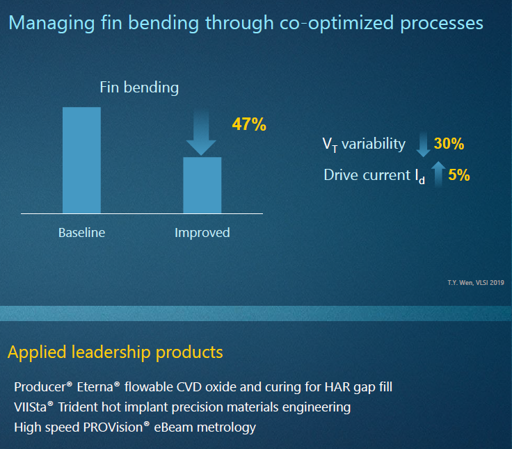
Figure 1: Applied’s co-optimized processes mitigate fin bending, resulting in 30-percent lower threshold voltage variability and an upwards of 5 percent increase in drive current.
Two HKMG logic elements—the interface and high-k layers—are key to boosting transistor drive current. However, neither layer has scaled since the 14nm node, creating a performance bottleneck. To address this, Applied developed a new Integrated Materials Solution (IMS™) that combines critical process steps in vacuum to permit a new degree of interface engineering and tuning. Using IMS™, we’ve demonstrated a new integrated gate stack that enables equivalent oxide thickness scaling to resume and improves drive current by 8 to 10 percent (see Figure 2).
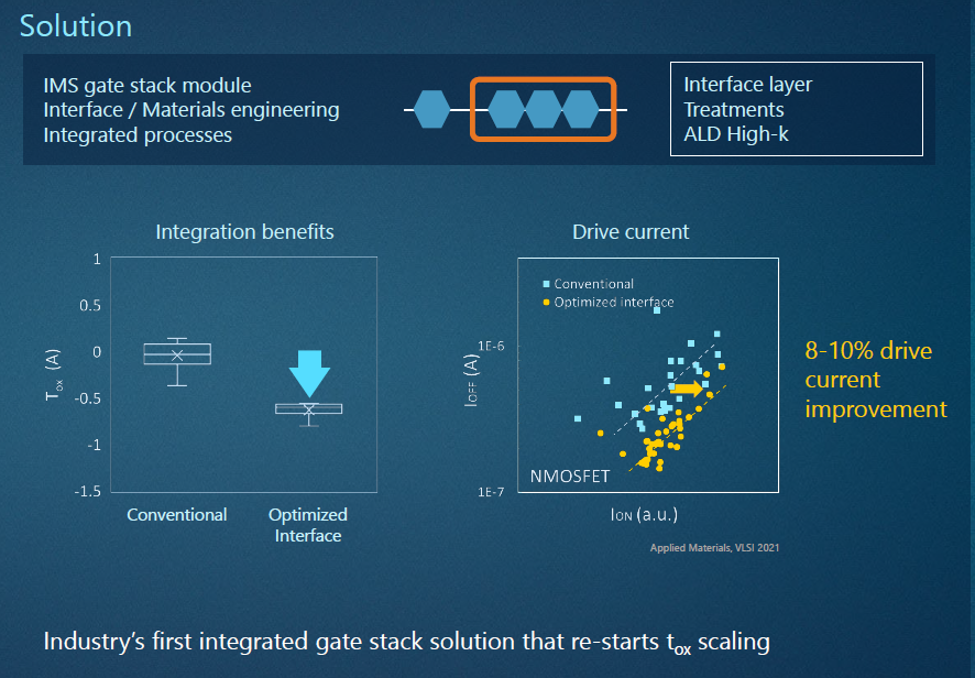
Figure 2: Using an Integrated Materials Solution, Applied has demonstrated a new integrated gate stack that enables equivalent oxide thickness scaling to resume and improves drive current by 8 to 10 percent.
In the transistor’s source/drain resistance module, scaling has reduced the contact area by 25 percent per node, causing an unsustainable increase in contact resistance. To counteract this, Applied developed a new co-optimized process technology that maximizes the area available for strain engineering (see Figure 3). The solution includes lateral etching that brings the embedded source-drain stressors closer to the channel. In addition, we developed a novel selective silicon arsenide (SiAs) epitaxial layer. The new material and materials engineering techniques lower resistance and increase drive current by 8 percent.
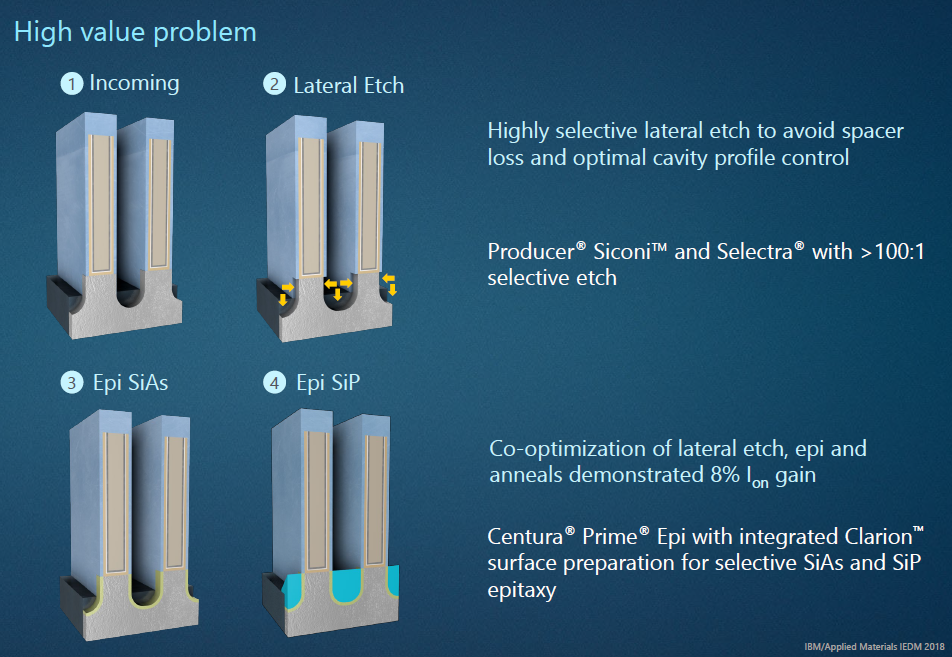
Figure 3: Applied’s solution to source/drain resistance consists of co-optimized etch, epi and anneals, resulting in an 8 percent gain in drive current.
Materials engineering innovations will become even more critical as the industry transitions from FinFET to the gate-all-around (GAA) transistor architecture for further improvements in performance and power (see Figure 4). In GAA, the transistor channel orientation shifts from vertical to horizontal, with gates surrounding the channels on all four sides instead of three. Controlling channel thickness is critical to performance and power: in the move from FinFET to GAA, channel thickness control shifts from lithography and etch for the tall, thin fins to epitaxy and selective removal in GAA as they offer highly controlled growth and reduced variability. GAA transistors also require inner spacers between the channels, and proper engineering helps reduce capacitance. The spacers are created with highly controlled, selective etching and gap fill processes. Metrology with eBeam can help ensure the new structures are properly and optimally formed to enable expected performance gains of 10 to 15 percent and power improvements of 25 to 30 percent.
Epi, selective removal and eBeam metrology are leadership areas for Applied Materials, and we are already developing co-optimized processes to help accelerate GAA solutions for customers. As a result, we expect to earn $1 billion in incremental revenue per 100K WSPM (wafer starts per month) in GAA compared to FinFET.*
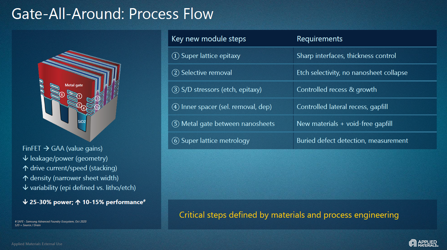
Figure 4: Materials engineering innovations will become even more critical as the industry transitions to the gate-all-around (GAA) transistor architecture.
Interconnect Scaling: New Integrated Materials Solution Reduces Via Resistance by 50 Percent
Interconnects consume nearly one-third of device power and account for more than 70 percent of resistive-capacitive (RC) delay. And unlike transistors whose performance improves with each process node shrink, interconnect wires encounter higher electrical resistance as they shrink, which in turn reduces performance and increases power consumption. Without a breakthrough, interconnect via resistance would increase by a factor of 10 from the 7nm to 3nm node, negating the benefits of transistor scaling.
To solve this challenge, Applied today introduced a breakthrough in materials engineering called the Endura® Copper Barrier Seed IMS™. This remarkable Integrated Materials Solution combines seven different process technologies in one system under high vacuum: ALD, PVD, CVD, copper reflow, surface treatment, interface engineering and metrology (see Figure 5). The solution eliminates a high-resistivity barrier at the via interface by replacing conformal ALD with selective ALD. It also includes copper reflow technology that enables void free gap fill in narrow features. The solution reduces electrical resistance at the via contact interface by up to 50 percent, improving chip performance and power consumption.
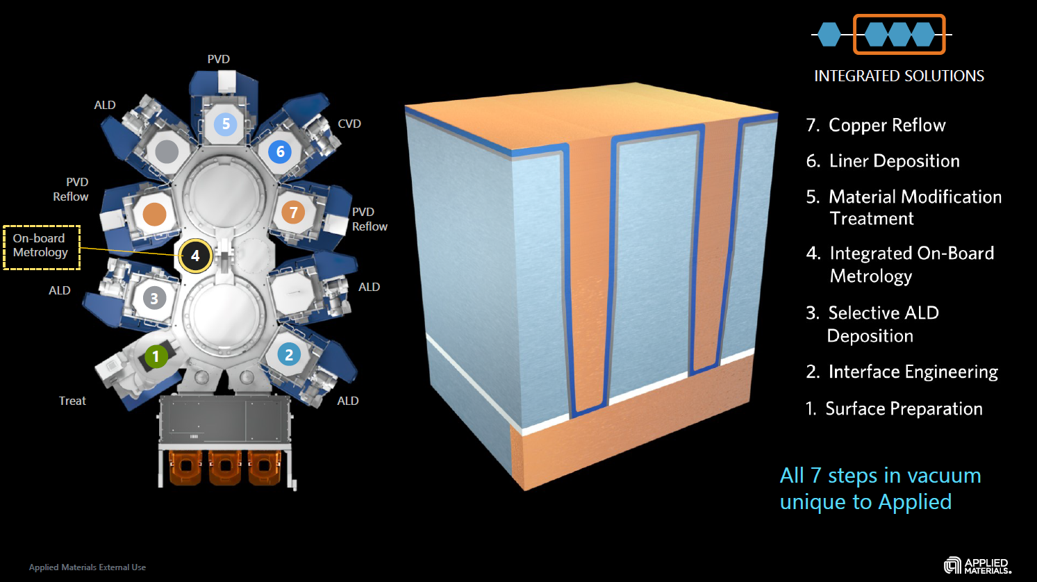
Figure 5: The new Endura® Copper Barrier Seed IMS™ combines seven different process technologies in one system under high vacuum to improve chip performance and power consumption.
Solving Pattern Variability with Innovations in Materials Engineering and DTCO
As EUV lithography is used in combination with multi-patterning techniques to create thinner lines, the issue of pattern variability is becoming increasingly problematic at smaller nodes. Instead of the straight, smooth edges we desire, we end up with increasing roughness and non-uniformity. In the past, this wasn’t a big concern because the features were much larger and the edge roughness was a smaller proportion. But as we continue to scale with EUV, features and edge roughness are becoming equivalent, resulting in stochastic defects such as open and short circuits.
In multi-patterning, the industry has typically used spin-on dielectrics and furnace steps to transfer the lithography pattern into the device layer. To reduce stochastic errors, we are replacing the spin-on dielectric with a high-quality CVD material that is co-optimized with our Sym3® etch system in a process monitored by our PROVision® eBeam metrology. In fact, we integrate CVD into our etch chambers. Once a wafer with rough features enters the chambers, we selectively deposit a thin layer of CVD material, tuning the process to deposit more material on wide openings and less on small openings, thereby correcting the distances between adjacent lines.
After deposition, we use a specially tuned etch mode that etches small features faster than large features, once again reducing the differences. Thus, by co-optimizing the CVD with our advanced etch technology, we can smoothen the lines and eliminate many of the stochastic defects. We also use eBeam metrology to quickly measure size variations in these tiny features. This co-optimized solution has been demonstrated to achieve a 50-percent reduction in local variation of the size of the features, a 30-percent reduction in line edge roughness, and a nearly 100-percent reduction in open circuit defects—which together enable continued logic scaling with healthy device yields (see Figure 6).
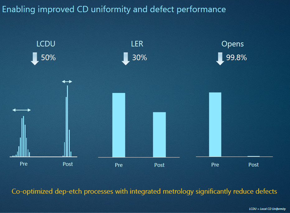
Figure 6: Co-optimization of Applied’s CVD with advanced etch technology eliminates many stochastic defects, resulting in major reductions in local critical dimension uniformity (LCDU), line edge roughness (LER) and open circuit defects.
The logic roadmap relies on continued logic density improvements to reduce area-cost. But 2D shrinking is slowing and becoming more difficult. There is less and less physical real estate available to continue pulling gates and wires closer together, and the closer they become, the worse the electrical challenges. Traditional Moore’s Law 2D scaling—a.k.a. pitch scaling or intrinsic scaling—has served the industry extremely well over the decades. However, looking ahead, pitch scaling will become increasingly supplemented with DTCO, which stands for design technology co-optimization (see Figure 7). DTCO allows logic designers to use clever 2D and 3D design techniques to increase logic density at the same pitch. A key upcoming inflection based on DTCO is the buried power rail with backside power delivery network. This new architecture routes thick power lines to the transistor cell from either the back side of the silicon wafer or from beneath the transistors, allowing further 2D scaling while simultaneously reducing voltage losses. Applied is helping enable this and other DTCO techniques with our expertise in metals, isolating dielectrics, etch and CMP processes.
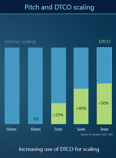
Figure 7: Design technology co-optimization (DTCO) is expected to deliver an increasing proportion of the overall scaling benefits in future nodes.
Closing Thoughts
Applied Materials aims to be the PPACt enablement company™ for our customers, and today’s Master Class illustrates how important materials engineering is to the future of logic scaling. For decades, the logic roadmap was driven by traditional Moore’s Law 2D scaling; however, as the benefit of this approach slows, the industry is supplementing it with a combination of techniques based on materials engineering to enable scaling to the 3nm node and well beyond. Customers are adopting a “new playbook for PPACt” which is creating substantial growth opportunities for Applied Materials. As logic transitions from 5nm to 3nm, Applied expects it served markets to grow between 25-30 percent.*
Another New Playbook lever for continued PPACt scaling in logic is heterogeneous design and advanced packaging, but we’ll save that conversation for our next Master Class which is targeted for September 8, 2021.
To learn more about the innovations I highlighted in this blog, please visit this page of our website where you can access the presentations and prepared remarks along with a video replay of the event.
*These are forward-looking statements, which are subject to risks and uncertainties. Factors that could cause actual results to differ materially from those expressed or implied by such statements include without limitation the risks and uncertainties described in our SEC filings, including our recent Forms 10-Q and 8-K. All forward-looking statements are based on management’s current estimates, projections and assumptions, and we assume no obligation to update them.
Tags: logic, scaling, interconnect, transistor, Patterning, PPACt, DTCO, IMS, gate all around, FinFET, EUV, 3nm
Uday Mitra, Ph.D.
Vice President, Engineering

Dr. Mitra is a Vice President of Engineering at Applied Materials. He has nearly 4 decades of experience in the semiconductor industry managing technology integration, lithography, etch, thin films and packaging modules for both logic and memory products. Prior to joining Applied in 2005, he was director of technology integration at Intel Corporation, where he spent 17 years holding various management positions. Uday received his Ph.D. in materials science from MIT and is a recipient of the Henry Marion Howe Medal from the American Society of Materials International.

Adding Sustainability to the Definition of Fab Performance
To enable a more sustainable semiconductor industry, new fabs must be designed to maximize output while reducing energy consumption and emissions. In this blog post, I examine Applied Materials’ efforts to drive fab sustainability through the process equipment we develop for chipmakers. It all starts with an evolution in the mindset of how these systems are designed.

Innovations in eBeam Metrology Enable a New Playbook for Patterning Control
The patterning challenges of today’s most advanced logic and memory chips can be solved with a new playbook that takes the industry from optical target-based approximation to actual, on-device measurements; limited statistical sampling to massive, across-wafer sampling; and single-layer patterning control to integrative multi-layer control. Applied’s new PROVision® 3E system is designed to enable this new playbook.

Breakthrough in Metrology Needed for Patterning Advanced Logic and Memory Chips
As the semiconductor industry increasingly moves from simple 2D chip designs to complex 3D designs based on multipatterning and EUV, patterning control has reached an inflection point. The optical overlay tools and techniques the semiconductor industry traditionally used to reduce errors are simply not precise enough for today’s leading-edge logic and memory chips.
