Products & Technologies
Products & Services
Contact
Products & Services
Products & Technologies
Services
Resources
Contact
Posted
June 15, 2021

Stay updated on our content.
Solving Pattern Variability is Critical to Further Scaling Advanced Logic Chips
by Regina Freed
Jun 15, 2021
As we prepare for the upcoming Applied Materials Logic Master Class, my colleagues Mike Chudzik and Mehul Naik wrote a pair of blogs that explore challenges to scaling logic transistors and interconnects. Here I will round out the Master Class discussions by examining issues in logic cell layout optimization and pattern variability which must be addressed to enable continued improvements in logic area-cost scaling, power and performance.
Shrinking Device Footprint with Design Technology Co-Optimization
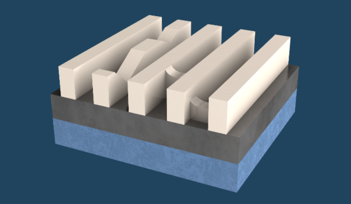
A logic device consists of very large numbers of individual logic cells that perform basic logical functions. Each cell has several transistor gates that are connected to one another by metal lines. In the vertical direction, the gates are separated by a distance we call the “contacted gate pitch.” In the horizontal direction, metal wires connect the gates to one another, separated by a distance we call the “metal pitch.” By multiplying these two pitches, we have a good measure of the area occupied by a single unit cell (see Figure 1).
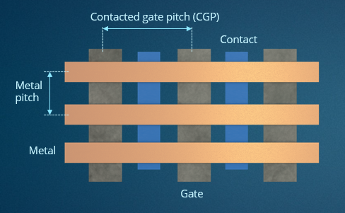
Figure 1: The contacted gate pitch and metal pitch are key parameters determining logic density.
Historically, the industry has scaled these cells using lithographic patterning to make the gates and wires thinner and bring them closer together. We call this pitch scaling or intrinsic scaling, and it has delivered incredible gains. However, as we continue to move to smaller process nodes, the physical real estate available to continue pulling gates and wires closer together is rapidly disappearing. At the same time, putting electrical devices and structures in such close proximity can cause signal interference which degrades device performance and power characteristics.
Applied is helping enable an additional scaling method that is gaining more attention because it is delivering an increasing proportion of the overall scaling benefits in future nodes. Known as Design Technology Co-Optimization (DTCO), it allows logic designers to use clever ideas along with new materials and materials engineering techniques to reduce area-cost without changing the lithography and pitch.
When I explain DTCO to my friends outside the industry, I make the analogy of remodeling a house. If the lot size is limited, then instead of shrinking the bedrooms to make space for an office or game room, we can add a second story or cellar. That may require additional materials and engineering—such as load-bearing supports to ensure structural integrity—or some excavating equipment. In a logic cell, DTCO allows us to put more features in less space by moving a critical element like a transistor contact from the side of the device to on top of the active area. That’s called “Contact Over Active Gate.” Other recent examples from the logic roadmap are “Single Diffusion Break” where dual insulating structures between adjacent transistors are replaced by a single, higher quality structure to save space. Each of these approaches has required creativity and some risk taking, mitigated by the use of higher-quality materials and more precise materials engineering techniques.
Customers expect DTCO to drive an increasing portion of logic scaling in emerging nodes, and I’ll discuss these applications at the Master Class.
Overcoming Pattern Variability
Pitch scaling can also continue if we can find ways to overcome a problem that greatly increases as we scale further: pattern variability. A special challenge of interest is combining EUV lithography with multi-patterning techniques to create thinner lines.
To achieve reliability and yields along with power, performance, area and cost (PPAC), we need to maintain edges that are straight and smooth. In reality, there is roughness and non-uniformity at the edges of every feature. In the past, this wasn’t a great concern because the edges represented a very small percentage of the feature width: we could largely ignore them. However, as we continue to scale with EUV, the edges can compose 30 percent of line width (see Figure 2). Now the edge roughness is critical. There is a growing trade-off between lithography resolution and line edge roughness. And the trade-off becomes especially critical as we increase the number of multi-patterning steps which can multiply the negative impacts of non-uniform edges.
The roadmap challenge is patterning defects that create electrical issues. In some places, edge variability on the two sides of the metal line creates features so skinny that we have a “pinch off” which creates an open circuit. In other places, edge roughness causes neighboring lines to become too close together, causing them to merge and creating a short circuit. Patterning engineers have a name for these problems: “stochastic” defects. They consume a lot of attention at technical conferences.
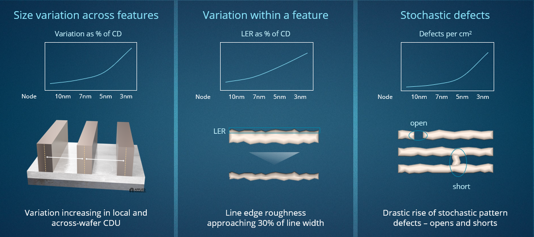
Figure 2: Key challenges in EUV patterning include local and across-wafer critical dimension uniformity (CDU), line edge roughness (LER), opens and shorts.
Fortunately, there are highly innovative new integrated materials solutions that work at the nano scale to help fix these stochastic issues and enable EUV double-pattering to succeed. I’ll cover them in detail during the Master Class.
In summary, advanced logic can continue to scale using both pitch scaling and DTCO. Applied Materials is already working closely with our customers to accelerate the next several logic nodes and provide chip designers with simultaneous improvements in power, performance, area-cost and time to market.
Tags: Patterning, multi-patterning, variability, scaling, logic, Design Technology Co-Optimization, DTCO, PPACt
Regina Freed
Vice President, AIx™ Solutions

Regina Freed has more than 20 years of experience in the semiconductor industry, managing semiconductor process and equipment development for both logic and memory processes, including co-optimization between deposition and etch, lithography, metrology, and defect inspection. At Applied Materials, Regina leads our AIx™ program that enables us and our customers to accelerate development and ramp through Actionable Insights as well as control our processes to deliver improved process windows, enabling customers to scale faster and at lower cost, while optimizing device performance.

Adding Sustainability to the Definition of Fab Performance
To enable a more sustainable semiconductor industry, new fabs must be designed to maximize output while reducing energy consumption and emissions. In this blog post, I examine Applied Materials’ efforts to drive fab sustainability through the process equipment we develop for chipmakers. It all starts with an evolution in the mindset of how these systems are designed.

Innovations in eBeam Metrology Enable a New Playbook for Patterning Control
The patterning challenges of today’s most advanced logic and memory chips can be solved with a new playbook that takes the industry from optical target-based approximation to actual, on-device measurements; limited statistical sampling to massive, across-wafer sampling; and single-layer patterning control to integrative multi-layer control. Applied’s new PROVision® 3E system is designed to enable this new playbook.

Breakthrough in Metrology Needed for Patterning Advanced Logic and Memory Chips
As the semiconductor industry increasingly moves from simple 2D chip designs to complex 3D designs based on multipatterning and EUV, patterning control has reached an inflection point. The optical overlay tools and techniques the semiconductor industry traditionally used to reduce errors are simply not precise enough for today’s leading-edge logic and memory chips.