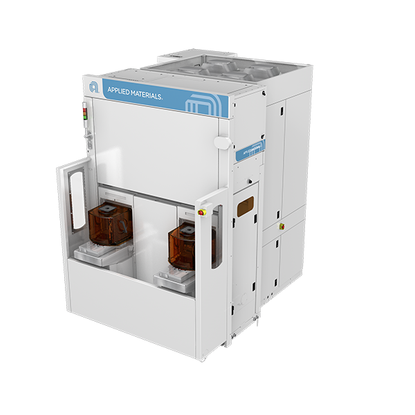
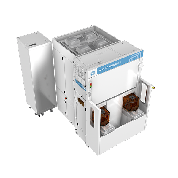
ComPLUS Optical Inspection
The ICAPS (IoT, communications, automotive, power and sensors) and mature logic markets continue to grow and require specialty devices that are traditionally manufactured using 90nm nodes or larger. However, intensifying competition is forcing fabs to innovate their processes and adopt sub-90nm nodes to stay differentiated and cost-effective. At smaller nodes under 90nm, fabs are challenged to use higher (and slower) inspection sensitivity to find smaller defects, while maintaining high throughput and low cost of ownership (CoO).
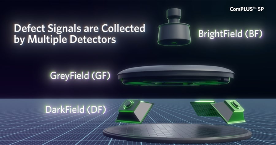
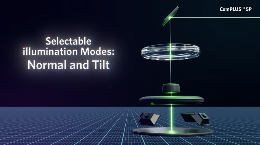
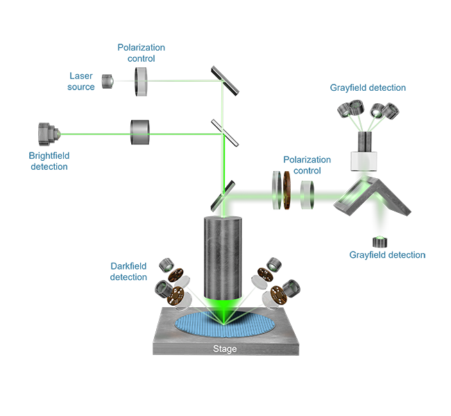
The ComPLUS™ 5P optical inspection system is optimized for process control in sub-90nm design nodes. Increased sensitivity is enabled by higher laser power, a photo multiplier tube, flexible illumination, polarization control and new inspection pixels—all critical features for maximizing signal-to-noise ratio and enabling the capture of yield-limiting defects. In addition, an upgraded image processor and stage, as well as simultaneous darkfield, grayfield and brightfield detection techniques, reduce CoO versus alternative solutions that employ multiple costly inspection passes to provide complete coverage. The ComPLUS 5P system addresses the emerging process control requirements of the ICAPS and mature logic markets by significantly reducing CoO and increasing inspection sensitivity.
- 1 / 4
- 2 / 4
- 3 / 4
- 4 / 4