Products & Technologies
Back to Menu
Products & Technologies
Services
Resources
DRAM Anatomy
Dynamic random access memory (DRAM) is a computer component where the processor goes to quickly store information needed to perform billions of calculations every second. A typical DRAM chip has three major areas:
- The cell array, where the individual bits are stored in tiny capacitors;
- The logic or core area, where devices such as sense amplifiers and word line decoders help determine how data is accessed from the cell array;
- The periphery, which forms the communication links in and out of the DRAM chip.
All three areas must scale to meet the industry’s ever-increasing DRAM performance requirements. These scaling requirements include maximizing the charge that can be stored in the capacitor, reducing sense amplifier variability, and reducing power losses due to the wiring in the circuitry.


Cell Array Scaling
The DRAM cell array where data is stored is the largest part of the die The density of the die can be increased by increasing the number of cells in a unit area. For this to happen, the dimensions of the cell capacitor and transistor must be reduced. This, in addition to the reduction in gate and bitline pitches, helps scale the DRAM cell.
The unique combination of our advanced DRACO® hard mask and Sym3® hard mask etch tool helps our customers achieve a 30% reduction in the thickness of the hard mask used for capacitor etch. In addition, we have been able to deliver a 50% reduction in variability of the diameter of the capacitor holes. This has helped reduce defects by over 100X.
Periphery Logic Scaling
Data in DRAM cells are managed by periphery logic devices. The periphery circuitry primarily consists of highspeed logic transistors and the wiring that connects the various parts of the DRAM. Maximizing signals to this circuitry is critical to maintaining the integrity of information stored in the DRAM cell.
Many DRAM manufacturers have been replacing the polySiON dielectric with a high-k material and the polysilicon gate with a metal gate to improve transistor performance. When several different films are deposited on top of each other, any defects in the films as well as interfaces play a big role in how the electron transport works.
Applied Materials offers an industry leading low-k dielectric product called Black Diamond® for DRAM backend copper wiring to efficiently address periphery logic scaling. Black Diamond offers a 25% reduction in dielectric constant. The reliability of the backend copper metallization has been improved over 10x by the adoption of our Endura CuBS product along with CVD Cobalt. The use of cobalt capping helps reduce copper electromigration at higher current densities.


DRAM Stacking – HBM
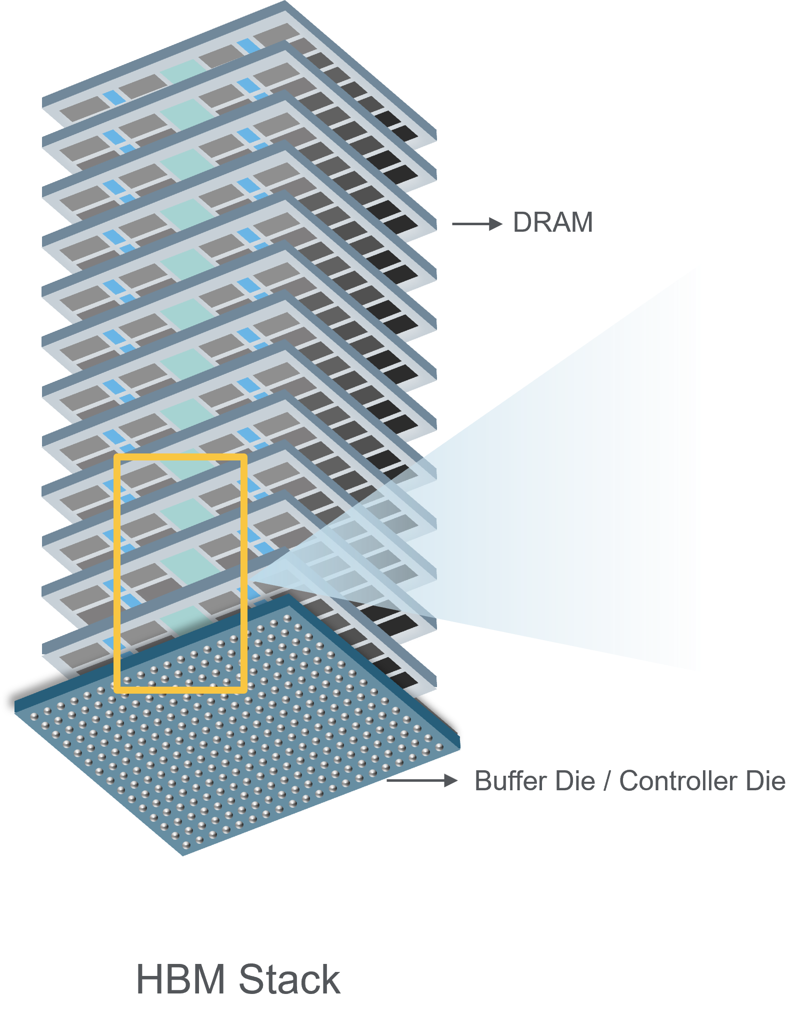
To provide the massive amounts of memory required for AI applications, chipmakers have turned to high-bandwidth memory (HBM) – a high-performance, low-latency architecture built from stacks of advanced DRAM. While innovation in DRAM chips is important, the density and bandwidth behind HBM is realized through advanced 3D packaging. Applied Materials is a leader in the materials engineering technologies needed to support the industry’s growing adoption of HBM. Learn more here.
Vertical Scaling – 3D DRAM
3D DRAM refers to the architectural storing of bits in the vertical direction, similar to 3D NAND. However, DRAM is almost 1000x faster than NAND and achieves this speed by using a high mobility silicon substrate as the starting material to form the channel. The high speed of DRAM also comes from a charge can be moved in and out of the capacitor quickly. As DRAM scales in the vertical direction, new material innovations are required to enable high mobility and ultra-low defect channels.
Applied Materials is a leader in new material innovation in technologies that are used to deposit high mobility materials, including epitaxial growth, PVD and ALD. Once deposited, these films are etched to access the bottom layers. 3D DRAM is expected to require advanced gap, selective removal and advanced doping capabilities. These capabilities must be integrated seamlessly to enable a successful solution. Our leadership in developing integrated materials solutions® to co-optimize these various processes will also be a key enabler to offer holistic solutions to integration challenges that 3D DRAM is bound to face.

