Products & Technologies
Products & Services
Company
Contact
Back to Menu
Products & Services
Products & Technologies
Services
Resources
Company
Contact
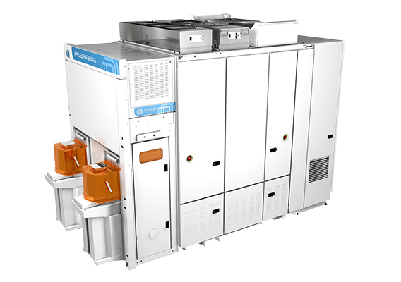
Vera Optical Inspection
As we move toward electronic products that are smarter and more connected, they require more specialty semiconductors built on mature process nodes. These applications require systematic defect detection to maximize yield, as well as latent defect detection to increase reliability, during chip manufacturing.
As part of Applied’s ICAPS (IOT, Communications, Automotive, Power and Sensors) product portfolio, the Vera® Bright-field patterned wafer inspection system offers non-leading-edge node chipmakers comprehensive wafer inspection options using a deep ultra-violet (DUV) laser source. The Vera system enables chipmakers to detect a wide range of defects, including latent reliability defects with high inspection sensitivity, at a low cost of ownership.
Based on the Enlight® platform’s unique architecture, the Vera optical system provides high resolution and best-in-class sensitivity with high-NA optics and dual channel detection (bright-field and grey-field lighting), as well as novel detection algorithms and enhanced productivity features. The Vera system also has advanced 3D polarization control to enhance defect signals and reduce noise. Vera is compatible with Applied’s ExtractAI® technology, enabling AI-based connectivity to Applied’s SEMVision® defect analysis tool. ExtractAI helps customers rapidly create fully classified noise-free maps during in-line monitoring.
Combining unique architecture, detection capabilities and productivity features, the Vera system helps fabs with mature process nodes improve product reliability with latent defect detection and drive towards zero defects, as well as provide comprehensive defect information for the following applications.
1. Critical patterning end of module inspection (etch and CMP)
2. Product ADI (after photoresist development)
3. Short loop ADI, PCM (portable conformal mask) and other lithography applications

- 1 / 2
- 2 / 2