Products & Technologies

Products & Services
Company
Contact
Back to Menu
Products & Services
Products & Technologies
Services
Resources
Company
Contact
Xi'an Center Advances More-than-Moore Techology Development
By Mike Rosa, Ph.D.
Applied Materials will soon mark its thirty-fourth year in China, where, since 1984, its operations have grown to include more than 1,600 full-time employees supporting sales, service, and a rapidly growing Global Development Center (GDC) located in the ancient capital of Xi’an (see Figure 1).
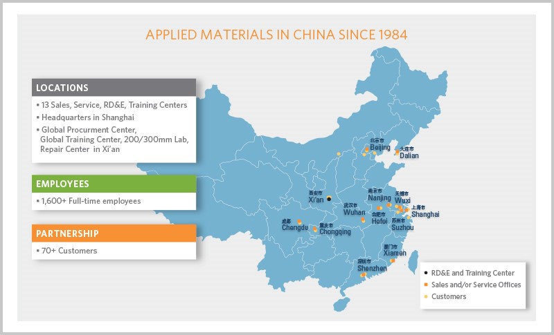
Figure 1 - Current Applied Materials operations in China.
The Applied Xi’an facility serves as a customer support hub for China, including procurement, training and repair operations. Additionally, it houses the GDC operation, which is the main research, development, and engineering (RD&E) operation for all More-than-Moore (MtM) applications for the Applied Global Services (AGS) Equipment Product Group (EPG), with a team of more than 20 specialized hardware and process engineers. (Figure 2)
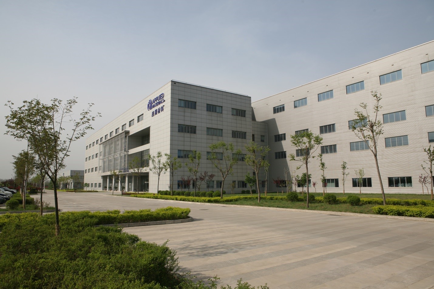
Figure 2 - Applied Materials’ Xi’an GDC is the hub for MTM technology development on legacy 200/300mm wafer processing equipment.
Legacy 300mm Processes
The Xi’an R&D projects mainly serve ≤200mm applications over the full range of PVD, CVD, Etch, CMP, Epitaxial (Epi) silicon, and Metrology tools. However, with the recent addition of a bridge-capable Deep Reactive Ion Etch (DRIE) tool, the team is now also able to conduct development for what is considered the legacy 300mm space, where the larger wafers are used for other-than-leading-edge processes, most often for MtM applications. The use of the larger wafer size is a trend we expect to see increase steadily over the next 2-3 years.
The Xi’an center’s ability to support customers’ needs on wafer sizes ranging from 100mm in diameter up to 300mm is indicative of the wide range of applications in the MtM space. Previous novel device technologies largely relied on unique processes based on chamber technologies such as DRIE. However, many of today’s generation of MtM devices are underpinned by new materials. And while the development of many of these new materials is on platforms such as PVD, CVD and Epi – there is a growing requirement that goes beyond the development of the unit processes.
With the growth of MEMS, power, wafer-level packaging and other MtM applications, there is considerable pull by customers around the world for new chamber technologies in the legacy equipment space.
New Technologies Developed in Xi’an
Today, on ≤200mm technologies, the Xi’an GDC supports the EPG technology roadmap in projects such as thick aluminum and thick silicon Epi deposition for power applications; piezo materials for a range of applications in consumer electronics; 5G communications; automotive; photonics; and wafer-level packaging. These are in addition to the numerous other technologies on CVD, CMP, and Etch being developed for the growing power device and MEMS markets. While the activity in these areas is rising, we are starting to see increased interest from customers toward 300mm wafers, which will require development of enhancements to legacy 300mm toolsets.
Leveraging the broad tool base in Xi’an, Applied Materials can add value beyond unit process development, proving out integration schemes that allow end-to-end processing. As more customers look to accelerate development times, it is often not enough to demonstrate unit processes in isolation: processes on either side of the material or process step need to be developed in an integrated fashion.
Wafer Level Packaging Increasing
Although this is always true for electrically active films, it is especially true for the growing wafer-level packaging (WLP) segment. As the use of WLP technology increases on ≤200mm and 300mm alike, more customers are looking for fully-integrated, end-to-end solutions, demonstrated on their wafers. (Figure 3.)
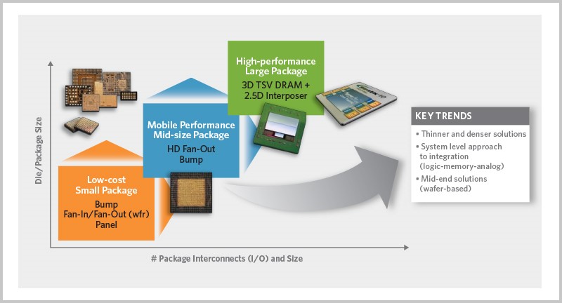
Figure 3 - Key trends in WLP packaging solutions.
To develop packaging schemes involving through-silicon vias (TSVs), under bump metallization (UBM), and solder bumps, wafers are processed both in the Xi’an GDC and at the Applied Materials Packaging, Plating and Cleans (PPC) operation in Kalispell, Montana, where electroplating development and demonstration is performed.
Many customers in the power, high brightness LED, and MEMS spaces are utilizing the WLP integration processes offered by EPG to develop their own 150mm and 200mm WLP solutions. Thus, Applied is able to help customers shorten their process development time, while demonstrating the capabilities of Applied toolsets.
More-Than-Moore Booming
What does the future look like for Applied Materials’ Xi’an development center? The semiconductor industry is booming globally, and China is no exception. The Xi’an GDC is seeing significant increases in engagements with both Chinese and international customers. And as global demand for MtM technologies continues to grow, the wafer size needs of the various segments will broaden as well.
For MtM RD&E, that means updating technology roadmaps from ≤200mm wafer sizes to 300mm wafers where possible. To accomplish this EPG relies on both the installation of legacy 300mm toolsets in Xi’an as well as collaboration with groups across the company, including the Office of the Chief Technology Officer (CTO) and the Advanced Process Technology Development (APTD) group.
The future looks bright indeed as the adoption of MtM technologies shows no signs of slowing and there is growing momentum behind the migration of road-mapped 200mm MtM technologies onto legacy 300mm toolsets.
For additional information, contact mike_rosa@amat.com.