Products & Technologies
Back to Menu
Products & Technologies
Services
Resources
Posted
August 27, 2024

Stay updated on our content.
Understanding the Inflection in Wafer Fab Equipment Growth
By Sundeep Bajikar
August 27, 2024
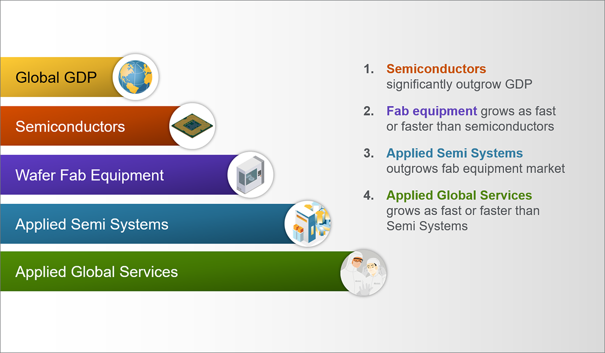
In my previous blog, I outlined a framework for why we at Applied Materials believe the wafer fab equipment (WFE) market can grow as fast or faster than the broader semiconductor industry. To better understand the context behind this expectation, I would like to take a look back at some of the critical factors that helped bring the WFE sector out of its long period of flat growth in the early part of this century.
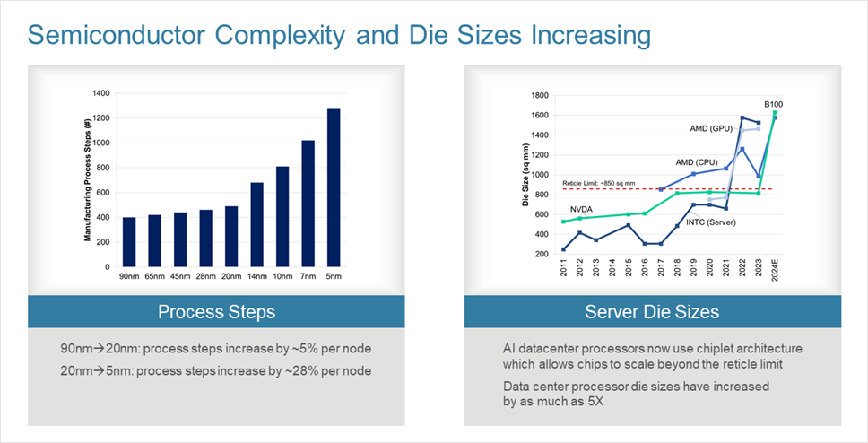
The transition took place in 2015, which corresponds with the beginning of the slowdown in classic Moore’s Law scaling – an important development that contributed to the positive inflection in WFE growth. Around the same time as transistors began shrinking at a slower rate, the number of steps needed to make a leading-edge chip began to increase, as can be seen in the chart on the left below. From the 90nm to 20nm generation, the number of steps increased at about 5% per technology node. This rate grew dramatically from 20nm to 5nm, with steps increasing at nearly 30% per node. Specifically, this timeframe saw the transition from 2D planar transistors to 3D FinFETs combined with the need to create new kinds of wiring to solve electrical resistance issues.
With transistor counts growing at a slower pace, chipmakers have begun to build bigger chips. The chart on the right below illustrates the point that we can no longer fit all the transistors we need for advanced server chips within the reticle limit, which is the 850-square-millimeter die size limit of lithography systems. It now takes more than one chip to make a high-end server processor.
Source: Evercore ISI Research; (1) Evercore ISI Research, electriiq.com, Applied Materials presentation; (2) company data, Evercore ISI Research, AnandTech, wccftech.com, techpowerup.com, Locuza
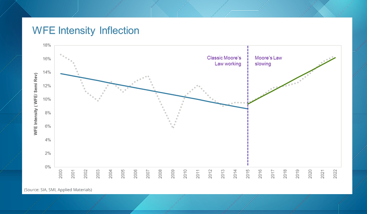
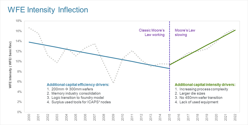
These factors had a profound impact on equipment capital intensity, which is a measure of the cost of equipment assets necessary to support a certain level of semiconductor industry revenue. Equipment capital intensity was around 17% in 2000 and declined to around 9% in 2015. During this period, classic Moore’s Law scaling was working nicely and the transition to larger 300mm wafers gave chipmakers a 125% increase in the number of like-sized chips on every wafer produced. At the same time, the memory industry consolidated and many logic makers transitioned to the foundry model, making both sectors more capital efficient. When these memory and logic chipmakers got out of manufacturing, their equipment was sold into the used equipment market and allowed ICAPS* chipmakers to buy equipment at a small fraction of the price of new equipment.
However, capital intensity began to increase from 2015 onwards. As I outlined earlier, this was when Moore’s Law began slowing, driving increases in process complexity and die sizes. In the past, when capital intensity increased in this way, a new wafer size would be introduced to help bring it down. During this period, the industry started to make a move to 450mm wafers, but it ultimately never materialized. This caused the growing ICAPS market to absorb all of the excess used equipment. This last point is very important. ICAPS typically drives 50% or more of total semiconductor industry revenue. When ICAPS chipmakers began purchasing new equipment instead of used equipment, their capital intensity increased by as much as a factor of three.
Source: SIA, SMI, Applied Materials; ICAPS includes foundry/logic spending at 10nm and above nodes.
At Applied, we believe this level of capital intensity can be sustained, causing the equipment industry to grow as fast or faster than the semiconductor industry on a through-cycle basis. The emerging IoT + AI era is creating a new wave of growth that we expect to drive continued high levels of equipment capital intensity.
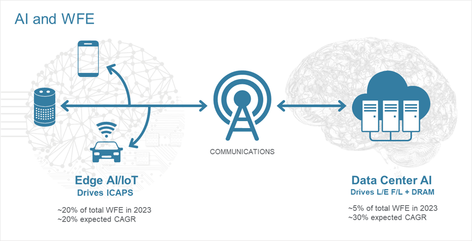
We see IoT and AI as two sides of the same coin, as depicted in the chart below. The left side creates and transmits data that can be understood and monetized, which happens today primarily on the right side. This is the biggest computing era yet, and it is projected to drive the semiconductor industry to $1 trillion dollars in annualized revenue by around the end of the decade. We believe the left side of this ecosystem drove around 20% of WFE in 2023, and the right side drove only around 5% of WFE. However, we expect growth rates in the coming years to be much higher, perhaps around 20% on the left side and around 30% on the right.
Source: Applied Materials analysis. Non-AI device segments include non-AI servers, smartphones, PCs, telecommunications equipment and televisions.
We believe these trends are going to drive meaningful inflections in semiconductor sales and WFE. Mobility in the form of smartphones and tablets has been the #1 end-market driver of leading-edge foundry-logic and DRAM wafer starts since 2010, with PCs #2 and data center #3. Given the growth in AI and the upcoming semiconductor inflections, we believe data center will cross over PCs within the next several years – and a few years later, data center could surpass mobility to become the #1 driver of leading-edge foundry-logic and DRAM.
It is important to note that year-to-year growth over shorter periods can be quite volatile. The approach we have taken to growth rates and capital intensity is to look at things on a through-cycle basis – over multiple business cycles. From this higher-level vantage point, we are confident in the long-term trajectory of the WFE sector.
In the following video, I share more about our approach to measuring performance over multiple business cycles, while also highlighting how the new IoT + AI era is driving a shift to more materials-enabled scaling – a topic I plan to unpack further in my next blog.

*IoT, Communications, Automotive, Power, Sensors
Sundeep Bajikar
Corporate Vice President, Corporate Strategy and Marketing

Sundeep is Head of Corporate Strategy and Marketing (CSM) and guides the executive leadership team in the development of the company's growth thesis, strategic priorities, key initiatives and investor communications. He is also responsible for developing Applied’s marketing capabilities and community. Sundeep’s work served as the foundation for Applied’s strategies related to AI, ICAPS, Heterogenous Integration and Net Zero.
He joined Applied in 2017 after spending ten years as a Senior Equity Research Analyst covering global technology stocks, including Apple and Samsung Electronics, for Morgan Stanley and Jefferies. Previously he worked for a decade as a researcher, ASIC design engineer, system architect and strategic planning manager at Intel Corporation.
Sundeep holds an MBA in finance from The Wharton School and M.S. degrees in electrical engineering and mechanical engineering from the University of Minnesota. He holds 13 U.S. and international patents with more than 30 additional patents pending. Sundeep is also author of a book titled, “Equity Research for the Technology Investor – Value Investing in Technology Stocks.” He was an Institutional Investor Rising Star.
Wafer Fab Equipment Positioned for a New Wave of Growth
At Applied Materials’ 2021 investor meeting, we suggested that the semiconductor industry had transitioned into a fourth major era of computing. This new “IoT + AI” era began in 2018, when machines generated more data than humans for the first time, complementing the markets for PCs and smartphones that defined the second and third computing eras. Each era creates a new wave of growth by effectively doubling the size of the industry, putting us on track to reach $1 trillion by the end of the decade, as suggested by multiple third-party forecasts.
How to Think About Rising WFE Intensity
WFE intensity increases primarily for two reasons: capacity and complexity. 1) Semiconductor fabs need more equipment to increase capacity so they can process more wafers and meet increasing demand for semiconductors. Conventional thinking is that capacity is the primary driver of WFE intensity. 2) Manufacturers add more wafer processing steps to produce more complex circuitry at higher levels of integration, thereby enabling more capable chips at a lower cost per function.

A New Normal for Semiconductor Growth?
Our analysis suggests semiconductor industry revenue growth inflected from a low-to-mid-single-digit CAGR in the 2000-2015 period to a mid-to-high-single-digit CAGR in the 2015-2021 period (see Chart 1). Based on our Battle of Exponentials framework and proprietary semiconductor industry model, we wouldn’t be surprised if semiconductor revenues continue to grow at this higher rate for the foreseeable future.
