Products & Technologies
Products & Services
Contact
Back to Menu
Products & Services
Products & Technologies
Services
Resources
Contact
Posted
May 20, 2024

Stay updated on our content.
HBM: Materials Innovation Propels High-Bandwidth Memory Into the AI Era
by Amulya Athayde and Ramesh Chidambaram
May 20, 2024
Nvidia’s CEO Jensen Huang famously referred to the launch of OpenAI’s ChatGPT as an “iPhone moment” for artificial intelligence, describing it as “one of the greatest things that has ever been done for computing.”[1] The Large Language Models powering today’s most advanced AI chatbots are estimated to have more than a trillion parameters – features that can be adjusted to optimize system performance – with future models expected to use an order of magnitude more. A massive amount of high-bandwidth memory (HBM) is required to support such large models and enable more energy-efficient AI training and inferencing. In fact, Huang has described HBM as a “technology miracle.”[2]
The need for HBM in high-performance AI has implications for the wafer fab equipment market. HBM made up only a modest amount of DRAM output in 2023 but is expected to grow at a 50-percent compound annual growth rate over the coming years. This is helping to drive healthy demand for DRAM wafer processing equipment and the associated capabilities needed to create HBM stacks. Applied Materials is the leading process equipment player in this space, with a broad range of enabling technologies for both leading-edge DRAM and 3D packaging.
A Legacy of Leadership
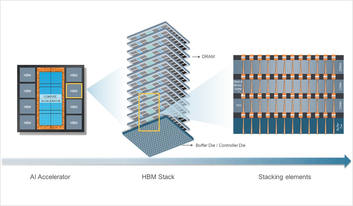
The primary components underpinning HBM are leading-edge DRAM chips. Today’s HBM stacks contain up to eight DRAM dies, with chipmakers planning to increase to 12 and beyond in the near future. At Applied, we have made strategic investments over the past decade to build and solidify our position as the industry’s leading provider of DRAM processing equipment. In 2023, our DRAM share was more than 10 points higher than it was a decade earlier, and our DRAM revenues were larger than our two closest process equipment peers combined. Our share of HBM packaging process equipment spending currently exceeds 50 percent.
We have deployed several innovations developed for logic to DRAM, to enable better density scaling and deliver significantly improved performance and power-efficiency. For example, memory manufacturers have recently followed logic chipmakers in adopting our high-k metal gate (HKMG) transistor technologies, which use exotic materials to improve gate capacitance and reduce leakage. This materials inflection in DRAM is being enabled by multiple Applied deposition technologies that help form the complex and delicate HKMG materials stack and fine-tune transistor performance. We have deployed similar innovations across other DRAM processing steps, including a new low-k dielectric material to overcome interconnect resistance challenges and a co-optimized CVD hard mask material and etch system to accelerate capacitor scaling.
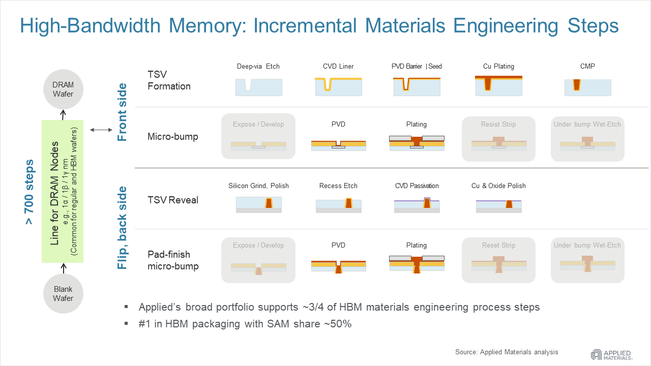
While innovation in DRAM chips is important, the density and bandwidth behind HBM is realized through advanced 3D packaging. The HBM manufacturing flow adds around 19 materials engineering steps to the approximately 700 process steps needed to make a conventional DRAM – and Applied serves about 75 percent of these steps with our equipment.
A critical ingredient in HBM DRAMs is through-silicon vias (TSVs) – vertical wires used to electrically connect the stacked chips. Applied was an early pioneer in TSV development. Nearly 15 years ago, Applied became a key collaboration partner with the European research organization imec to formulate the industry’s first TSV process flow and integration scheme. The collaboration led to the creation of the TSV standards used in HBM today.
Since that milestone, Applied has developed several additional, unique solutions for TSVs and other HBM packaging steps. These technologies take full advantage of our deep capabilities in chip interconnect wiring, leveraging several front-end wafer processing equipment technologies to enhance the back-end packaging steps needed to build HBM stacks. Our strength as the industry’s #1 provider of processing equipment for advanced packaging has helped us build our leadership position in HBM. In fact, we expect our HBM packaging revenues to grow by as much as 6X in fiscal 2024, growing to more than $600 million.
A Broad Packaging Portfolio
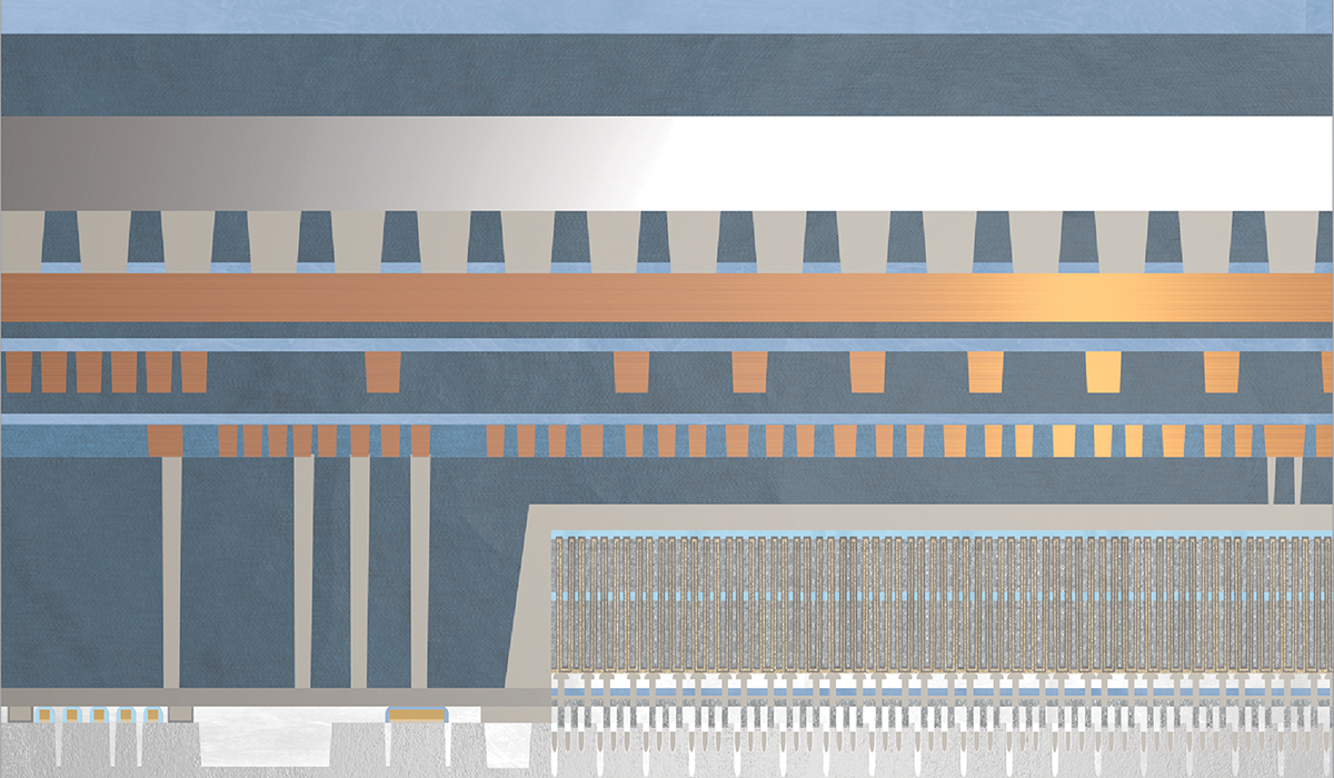
As highlighted earlier, HBMs require around 19 incremental materials engineering steps. On the front side of the wafer, 10 HBM steps are needed to create frontside interconnect pillars and TSVs, which are formed by etching trenches into silicon and then filling them with insulating liners and metal wires. After the frontside wafer processing is completed, the wafer is flipped for backside processing, with a further nine materials engineering steps needed to reveal the TSVs and create backside interconnect pillars.
The primary technical challenge with TSVs comes from the need to create and line high-aspect– ratio trenches while observing low thermal budgets. To address the need for higher HBM memory capacity and data bandwidth, the industry will be transitioning to new generations of devices with twice as many TSVs. As the TSVs become increasingly narrow, deposition uniformity variations become increasingly problematic, degrading both performance and yield.
Applied has developed dielectric and metal deposition technologies that enable higher-aspect-ratio TSVs and provide better coverage within via trenches. Our Producer™ InVia™ 2 CVD system uses a propriety process that enables low-temperature deposition of a uniform dielectric liner that precisely follows the geometry of the via sidewalls. Similarly, our Endura™ Ventura™ 2 PVD system increases the control of metal deposition to ensure good coverage of the barrier-seed layers, which delivers higher electrical performance and reliability.
Besides TSVs, micro-bump pillars are critical to the electrical and thermal performance of HBM stacks. While there has been significant innovation in reducing both the dimension and pitch of micro-bumps, contact resistance grows exponentially as these bumps and their corresponding bond pads shrink in size. The combination of our unique Volaris™ preclean technology and our industry-leading under-bump metallization PVD helps reduce contact resistance and parasitic power while improving bump reliability. In conjunction with Applied’s Nokota™ ECD plating tool, we have significant positions for micro-bump fabrication at leading customers.
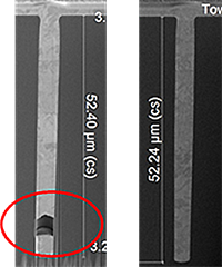
Left: If the PVD barrier-seed doesn’t have good coverage, then the downstream plating-fill step will see voids. Right: Ventura 2 ensures good coverage even with higher aspect ratios.
Another growing challenge with HBM processing is the stacking of very thin dies, which can be impeded by die warpage and bowing. Our Producer™ Avila™ PECVD system deposits a thin dielectric film on the back side of the wafer at low temperature, allowing chipmakers to control warpage by modulating the stress of the film.
Overall, Applied carries the industry’s most comprehensive portfolio of differentiated products for HBM manufacturing.
Enabling the Future HBM Roadmap
The relentless march of progress in AI compute will require continued innovation in HBM technology. To enable higher-density connections and lower latency, the next generation of HBM TSVs is expected to shrink from the current 5 µm diameter standard to 3 µm and below, resulting in higher aspect ratios. We have proven that our tool set is extendable to shrinking dimensions and more extreme aspect ratios by demonstrating electrical performance for various TSV dimensions.
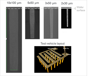
Applied has demonstrated electrical performance for a variety of TSV dimensions.
These roadmap demonstrations take advantage of the unique capabilities in our Advanced Packaging Development Center in Singapore – a state-of-the-art cleanroom that is among the most advanced wafer-level packaging labs in the world. It houses the industry’s only integrated TSV and micro-bump line, which features nearly 100 tools to run test vehicles in collaboration with customers. The center was established as a joint lab partnership with the Institute of Microelectronics (IME), a leading R&D institute of Singapore’s Agency for Science, Technology and Research (A*STAR).
With these deep R&D capabilities and the broadest equipment portfolio for HBM processing, Applied is well positioned to help chipmakers solve unique challenges in the HBM integration flow and continue to drive the roadmap for the future. Our holistic approach allows us to accelerate learning for customers and assure a smooth transition from R&D to volume production.
[1] UC Berkeley, Haas School of Business, Dean’s Speaker Series, January 21, 2023
[2] Nikkei Asia, March 20, 2024
Amulya Athayde
Senior Director of Strategic Marketing, Heterogeneous Integration Business Unit

Amulya Athayde is Senior Director of Strategic Marketing in the Heterogeneous Integration business unit at Applied Materials, responsible for product and business strategy. He has worked in the field of semiconductor fabrication since 1995 and has been involved in the development and commercialization of plasma etch, thermal deposition and wet clean process equipment. Amulya has a Ph.D. in chemical engineering from the University of Notre Dame and a Bachelor of Technology degree in chemical engineering from the Indian Institute of Technology, Bombay.
Ramesh Chidambaram
Senior Director of Strategy and Marketing, Semiconductor Products Group

Ramesh Chidambaram is Senior Director of Strategy and Marketing in the Semiconductor Products Group at Applied Materials, where he supports strategy formulation and related insight generation on topics across the breadth of Applied’s semiconductor portfolio. He started his career as an integrated circuit design engineer and has since held roles in equipment product development, marketing, operations and early-stage R&D programs. Ramesh has a MSc in electrical engineering from the Delft University of Technology and an MBA from the Rotterdam School of Management, Erasmus University.
Applied Materials Showcases Memory Innovations at IMW 2024
Large language models (LLMs) have been around for years, but they only recently entered the popular lexicon with the launch of ChatGPT and the ensuing generative AI boom.
Building on an Unmatched Foundation of CVD Innovation
Applied Materials recently celebrated the shipment of our 10,000th CVD system. For more than 30 years, Applied has introduced a steady stream of product and material innovations that have transformed the CVD semiconductor equipment market.

Applied Materials Earns Intel’s 2024 EPIC Distinguished Supplier Award
Applied Materials has earned Intel’s EPIC Distinguished Supplier Award. Through its dedication to Excellence, Partnership, Inclusion and Continuous (EPIC) quality improvement, Applied has achieved a level of performance that consistently exceeds Intel’s expectations.