Products & Technologies
Products & Services
Company
Contact
Back to Menu
Products & Services
Products & Technologies
Services
Resources
Company
Contact
Posted
November 06, 2019

Stay updated on our content.
Enabling the AI Era of Computing – Part 2

Nov 06, 2019
Welcome to the second piece in our blog series examining how the computing industry can work in new ways to enable the AI Era.
In our first blog, my colleague Ellie Yieh described the enormous opportunities and challenges facing the industry as we enter a new decade, and she offered a path for accelerating innovation—from materials to systems—based on a “New Playbook” for driving improvements in chip PPAC (performance, power and cost). She also talked about how the New Playbook requires a level of industry collaboration whereby engineers from across the computing industry think beyond our primary disciplines to maintain and accelerate the pace of innovation in a world that can no longer rely on the progress associated with classic Moore’s Law scaling. In particular, I want to flesh out the idea of “codesign” that Google’s Cliff Young talked about at the AI Design Forum in July.
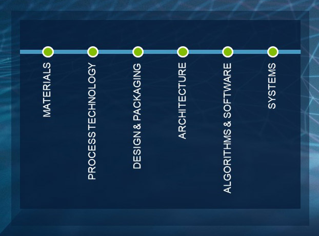
I’ll start by explaining what’s driving the need for codesign. Until recently, serial interaction between siloed parts of the industry (as shown in the graphic below) was adequate because Moore’s Law scaling drove exponential improvements in computing capability at a predictable, two-year cadence. Doubling the number of available transistors fueled improvements in PPAC, which enabled more sophisticated microarchitectures and algorithms and more powerful hardware and software systems. However, a consensus is growing that the siloed structure that produced the computing eras of the past—mainframe/minicomputer, PC/Internet, mobile/social media—will not be sufficient to fuel the IoT/Big Data/AI Era. As Cliff Young said, codesign from materials to systems will be needed to enable the AI Era.
One major consideration is less talked about: even if the exponential progress associated with Moore’s Law could continue, it would fall far short of the voracious appetite of AI. Since 2012, the compute needs of the large AI training models has been doubling every 3.5 months! This means that through this year, the needs of AI have grown about 8 million times—versus an expected Moore’s Law gain of only about 6X.
To keep up with these needs, the industry has made some important changes in architecture to better accommodate AI’s massive data sets and unique algorithms. In addition to using CPUs, we’ve adopted and adapted GPUs and also moved in the direction of customization with FPGAs and ASICs.
True codesign for AI involves an industry-wide focus on the unique characteristics and needs of AI and a willingness to break away from the architectural artifacts of previous computing eras. If we started our chip designs with a clean sheet of paper, we might design out branch prediction engines and high-precision floating-point math units that made sense in the past but waste space and power in AI. We would prioritize data bandwidth, avoid power-sapping inter-chip data transfers and prioritize energy over speed. Given the advantages of parallelism and low power over precision and serial speed, we might even look to neuro-inspired, analog computing.
These big leaps in architectural opportunity allow us to reconsider our basic assumptions about the materials and switches used to make calculations and store weights. We can explore with new degrees of freedom and the potential for radical improvements in key AI metrics like TOPs/watt, Frames/Joule and model prediction accuracy. This is what we mean by codesign, from materials to systems.
In fact, codesign is beginning to take hold, and industry dynamics are beginning to change as leaders in cloud and edge computing race to develop new architectures and chip designs optimized for AI. Companies including Amazon, Apple, Facebook, Google and Microsoft now have in-house chip design teams. They’re active in shaping new and emerging standards in areas like wireless networking, high-bandwidth memory and server interconnects, no longer satisfied with what’s on the shelf. They’re participating in SEMI events to learn more about what’s happening in materials and manufacturing, and SEMI is linking arms with EDA organizations to strengthen the ties between manufacturing and design.
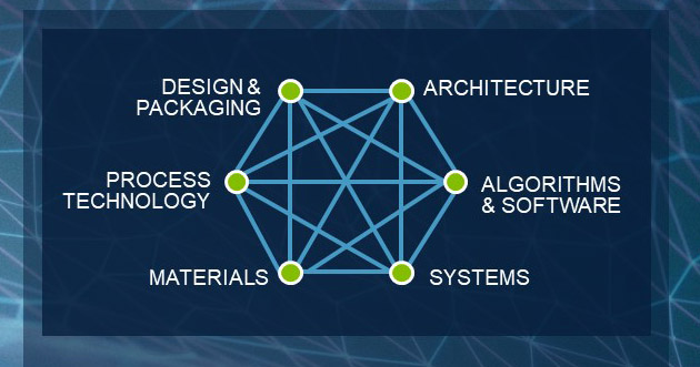
In 2018 and 2019, Applied Materials hosted an event called, “AI Design Forum—The Future of Computing from Materials to Systems.” There, we used the graphic below to represent the opportunity for a New Playbook that emphasizes codesign and parallel innovation over siloes and serial innovation. In keeping with the AI theme, we called it a “neuromorphic approach.”
When engineering team members meet to design something new, they are faced with tradeoffs. They can prioritize certain things—high performance or low power consumption, for example—and sacrifice others.
The codesign concept expands the disciplines that can interact to solve a problem, from materials engineers to the data center architects. Codesign increases the opportunities that can be brought to bear, and it encourages more creative outcomes.
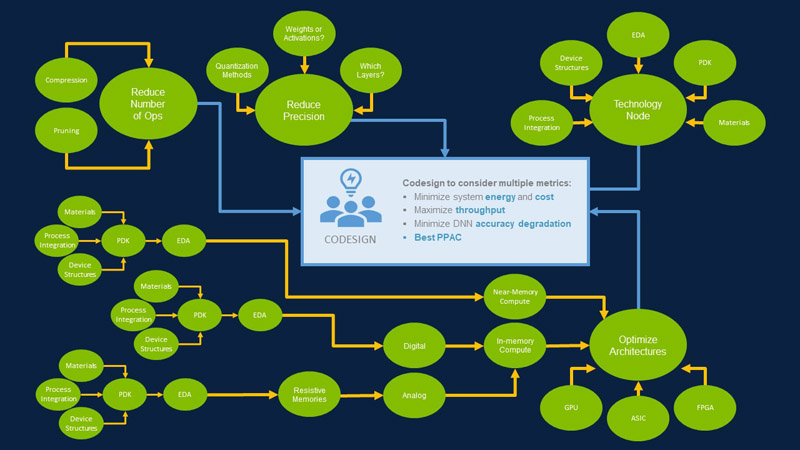
For today’s AI and machine learning, codesign is the only way to address all the relevant issues that will define the long-term success of this new era. Those in the semiconductor disciplines need to think beyond the relentless pursuit of PPAC to also consider:
- Training vs. inferencing
- Time to train
- Inference accuracy requirements
- Optimizing for the edge vs. the cloud
- Architecture choices to address “memory wall” bottlenecks
- Digital vs. analog compute
- Near-memory vs. in-memory compute
- Domain-specific vs. general-purpose architecture
- Suitability of new materials to neuromorphic systems
- And more as illustrated in the graphic below.
A special topic for making multidisciplinary codesign practical is the “Proof of Concept.” Innovations in chip materials and structures are far removed from the abstract world of system and chip architecture, design and modeling. Accelerating the practical use of any promising new material or on-chip logic or memory element requires developing both physical models and simulation models—in parallel (see figure below). These models provide calibration points throughout the innovation cycle and facilitate bridging the interdisciplinary gaps.
This modeling also helps in assessing the commercial promise of new ideas for specific applications and markets (such as automotive) before the first prototype exists in hardware, and well before the first prototype is piloted in a test fab prior to high-volume production.
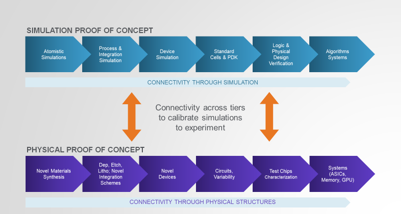
Simulation and fabrication are two technically distinct paths, aimed at the same result. A simulation proof of concept is much less expensive to create than a physical proof of concept, but at some point, pilot fabrication is needed to expose unexpected characteristics that need to be refined to prepare for smooth and profitable high-volume manufacturing of a commercial product. Given the high costs of modern chip fabrication, there is little capacity available in the industry for physical proof of concept work on codesigned innovations. To enable the AI Era, the industry will need a new type of facility where engineers from different disciplines can work side-by-side to accelerate innovation. We’ll take up this critical gap in the third and last installment of our blog series.
Tags: Codesign, AI, Moore's Law, chip design, materials engineering, AI Design Forum, machine learning
Buvna Ayyagari-Sangamalli
Head of Design Technology

Buvna Ayyagari-Sangamalli heads the Design Technology team at Applied Materials. With a career in various roles from Design Engineering to development of Customer IP Subsystems, she is intimately familiar with design challenges. At Synopsys she played a pivotal role in growing the IP business, where she led the IP Applications Engineering team and launched Customer IP Subsystems for AI, Automotive, IoT and other segments. Prior to that, she played a critical role in defining low-power EDA design methodologies. At Intel she worked on various mobile, desktop and processor chips. Her well-rounded 20 years in the semiconductor industry straddled architecture, design, EDA and IP.

Now is the Time for Flat Optics
For many centuries, optical technologies have utilized the same principles and components to bend and manipulate light. Now, another strategy to control light—metasurface optics or flat optics—is moving out of academic labs and heading toward commercial viability.

Seeing a Bright Future for Flat Optics
We are at the beginning of a new technological era for the field of optics. To accelerate the commercialization of Flat Optics, a larger collaborative effort is needed to scale the technology and deliver its full benefits to a wide range of applications.

Introducing Breakthroughs in Materials Engineering for DRAM Scaling
To help the industry meet global demand for more affordable, high-performance memory, Applied Materials today introduced solutions that support three levers of DRAM scaling.