Products & Technologies
Products & Services
Contact
Back to Menu
Products & Services
Products & Technologies
Services
Resources
Contact
Posted
July 12, 2019

Stay updated on our content.
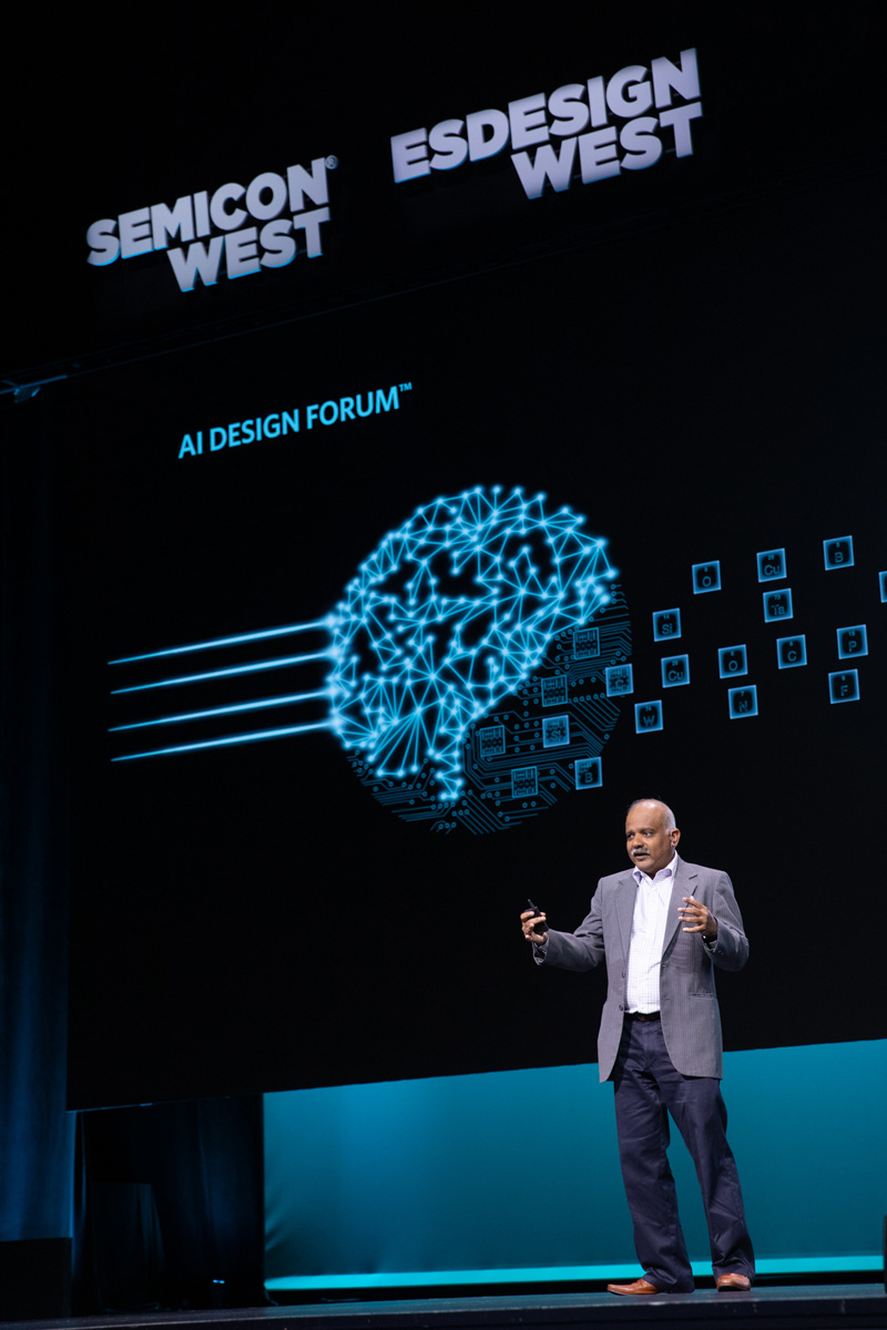
Highlights from a Successful #AIDesignForum 2019
Jul 12, 2019
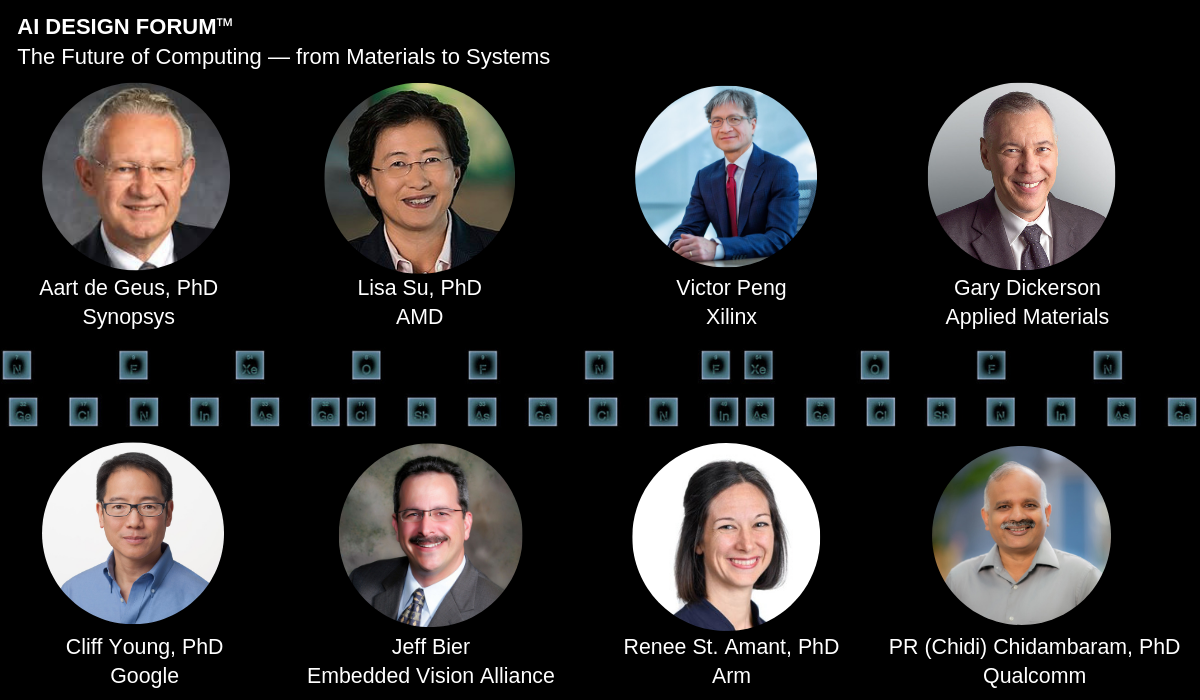
Leading technology CEOs and industry thought leaders from across the computing ecosystem convened in San Francisco earlier this week at the second AI Design Forum™ to discuss the future of computing—from materials to systems. What was made clear from the thought-provoking keynotes and many sideline discussions is that AI and Big Data create tremendous growth opportunities for the industry, but to realize their potential requires new levels of innovation. At the same time, classic Moore’s Law scaling is becoming increasingly challenged. The two-dimensional scaling techniques that drove Moore’s Law for the past 40 years are no longer delivering simultaneous improvements in performance, power and cost. The industry needs a new playbook for semiconductor design and manufacturing to drive innovation in the AI Era.
Another key theme that emerged from the event is the need for new types of collaboration and co-design across the ecosystem. This is critical to accelerating innovation as the industry races to bring new chip architectures, devices and computing systems to market. For decades the industry has operated in a serial fashion where degrees of separation exist between materials innovation and chip makers and system designers. We need to shift this approach and start working together in parallel in order to enable higher performance, more efficient computing. This is where events like the AI Design Forum, hosted by SEMI Americas, the Electronic System Design Alliance and Applied Materials, can help by bringing together leaders and technology experts from different domains to share ideas, discuss solutions and find new ways to work together.
We will be discussing more takeaways from the event in future blogs. In the meantime, we put together the recap below of the AI Design Forum on Twitter to share a taste of some of the insightful commentary and opportunities for collaboration coming out of the event. You can also access Applied Materials CEO Gary Dickerson's presentation materials.
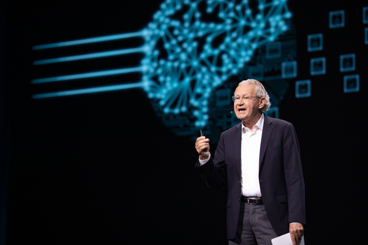
Aart de Geus, CEO of Synopsys, kicked things off with a very insightful presentation on the industry’s foundational role in enabling AI and how the fusion of silicon and software will open up the door to advanced computing.
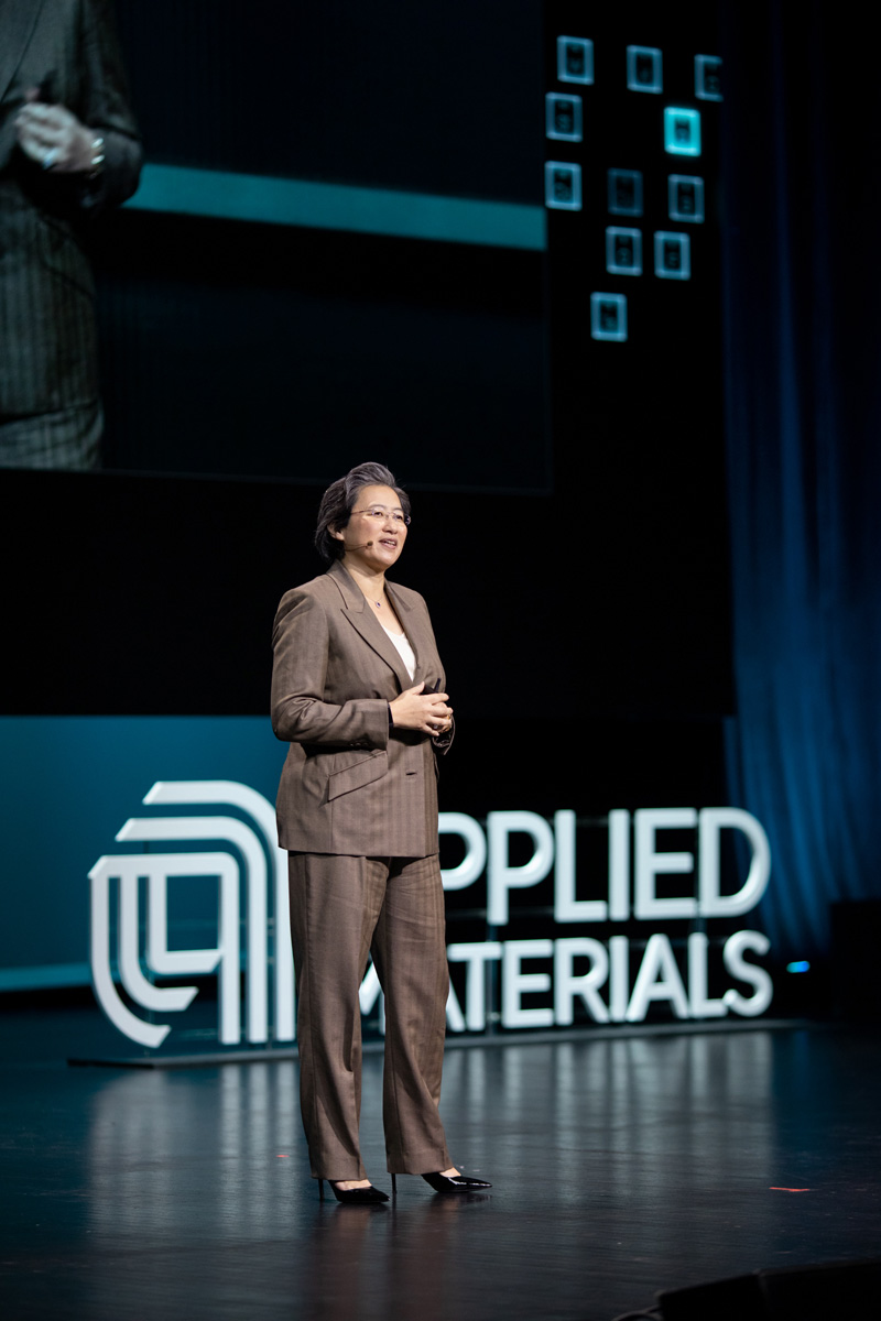
Lisa Su, CEO of AMD, explained why a very rich ecosystem is necessary to accomplish the full potential of machine learning and AI, and how heterogeneous platforms on open software must work across the industry.
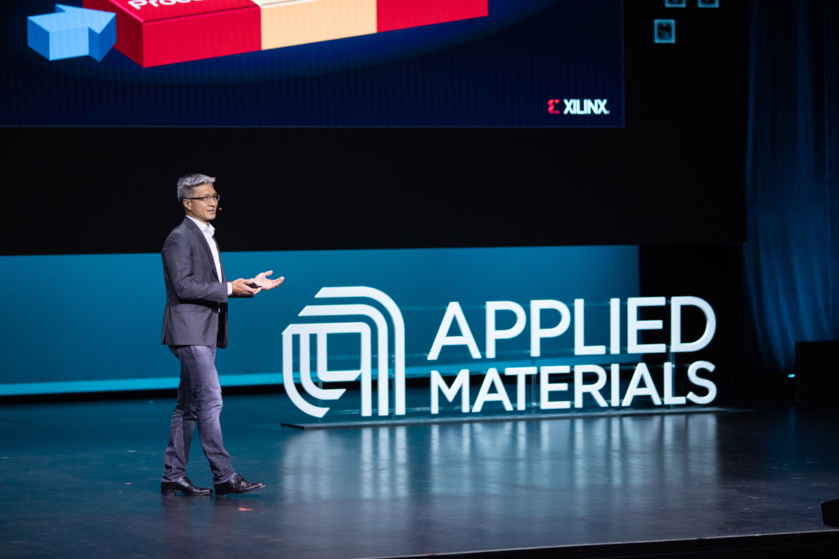
Victor Peng, CEO of Xilinx, shared how the next wave of advanced computing is all about architecture and distributed adaptable platforms that will meet the needs of future innovators.

Our CEO Gary Dickerson gave insights on why new computing approaches are needed to unlock the value of big data, and how the industry won’t get there by doing what we’ve done in the past. We need to drive innovation in very different ways!
Cliff Young from Google explained why collaborating across the ecosystem is crucial to accelerating the roadmap for creating even more valuable TPUs.
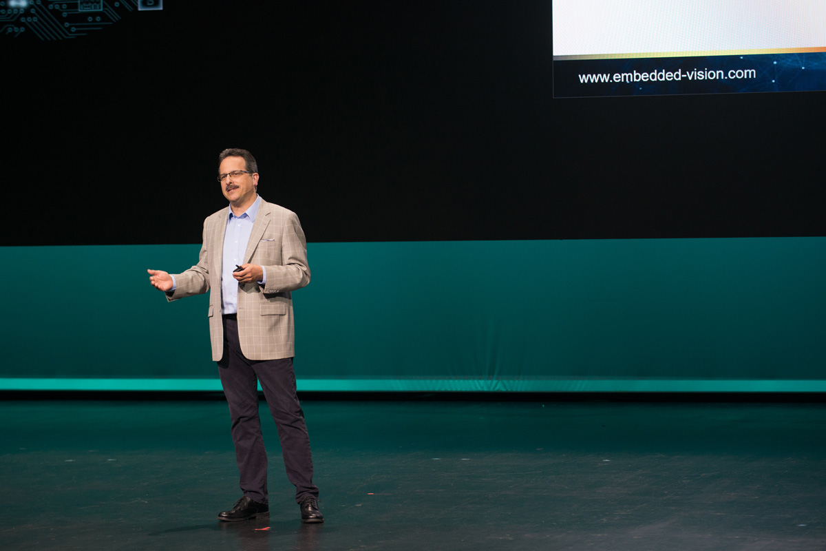
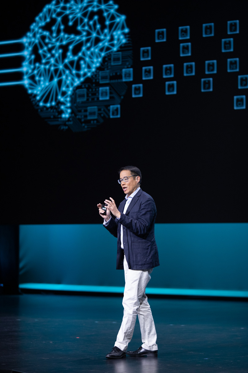
Jeff Bier from the Embedded Vision Alliance said the convergence of big data, deep learning and specialized processors is creating a once-in-a-generation opportunity. If you aren’t already thinking about how to benefit from this sea of change in tech, then now is the time.

Renée St. Amant from Arm said machine learning has opened the door to many vectors of innovation. We need to expand our frame across the stack and also into the future to help create what’s possible.
PR (Chidi) Chidambaram from Qualcomm closed out the forum by explaining what it will take to develop the 5G AI era and opportunities to improve power efficiency with in-memory computing.
Tags: AI Design Forum, AIDF, internet of things, iot, cloud computing, 5G, AI, artificial intelligence, machine learning, Big Data, deep learning, AMD, Arm, Embedded Vision Alliance, Google, Qualcomm, Synopsys, Xilinx
Applied Materials
Corporate Communications
The Applied Materials team publishes posts of general interest to our readers.

Now is the Time for Flat Optics
For many centuries, optical technologies have utilized the same principles and components to bend and manipulate light. Now, another strategy to control light—metasurface optics or flat optics—is moving out of academic labs and heading toward commercial viability.

Seeing a Bright Future for Flat Optics
We are at the beginning of a new technological era for the field of optics. To accelerate the commercialization of Flat Optics, a larger collaborative effort is needed to scale the technology and deliver its full benefits to a wide range of applications.

Introducing Breakthroughs in Materials Engineering for DRAM Scaling
To help the industry meet global demand for more affordable, high-performance memory, Applied Materials today introduced solutions that support three levers of DRAM scaling.