Products & Technologies
Products & Technologies
Services
Resources
Posted
September 26, 2024

Stay updated on our content.
Bringing eBeam Review to Compound Semiconductors

By Neta Shomrat
September 26, 2024
The power electronics industry has seen a resurgence in the past two decades – driven first by the advent of specialized power management chips for smartphones and tablets, and more recently by the major global transition to renewable energy sources and electric vehicles. At the heart of this transition lies the power semiconductor device, which modulates the flow of electrical energy to suit the demands of the application.
Silicon has traditionally been the material of choice for power semiconductors, but in recent years compound semiconductors such as silicon carbide (SiC) have enabled a new generation of power devices with superior performance. As a material, SiC is inherently harder than silicon with natural crystallographic defects that can cause chip performance, reliability and yield issuesAdvanced materials engineering is needed to manufacture SiC chips with minimum damage to the crystal lattice.
Applied Materials offers the industry’s broadest portfolio of specialized equipment for compound semiconductor manufacturing, including systems for deposition, etch, implant, chemical mechanical planarization and process control. At the upcoming 2024 International Conference on Silicon Carbide and Related Materials (ICSCRM 2024) in Raleigh, N.C., we will highlight our SiC portfolio and showcase new solutions to the unique challenges our customers face as compound semiconductors grow in popularity and sophistication.
Identifying and Characterizing New Types of Defects
Wafers made from compound semiconductors such as SiC have unique properties relative to silicon wafers. Not only are the underlying substrates harder and thinner – requiring alternative wafer handling techniques – but they are also prone to developing new types of crystalline defects during the creation of the bare wafers. These wafers are completed with epitaxy, whereby high-quality crystalline layers of SiC are grown on top of a SiC substrate. During the epitaxial SiC crystal growth, faults and dislocations in the crystalline lattice can occur.
The growth of compound semiconductors brings a new set of challenges for metrology and defect inspection – a vital set of fab solutions that monitor and control the quality of individual manufacturing steps. Defect control is a major priority, and chipmakers rely heavily on wafer inspection techniques to help find and correct yield-killing defects quickly.
These defects degrade the reliability and performance of power electronics devices, and they have negative impacts on yield. As they move through the process steps required to build circuits, wafers are exposed to high temperatures and mechanical stresses that can turn a minor one-dimensional dislocation in the lattice to larger, yield-limiting defects. That’s why it is important to accurately characterize the crystal defects and identify their severity to the device, while monitoring their progression through the entire fabrication process.
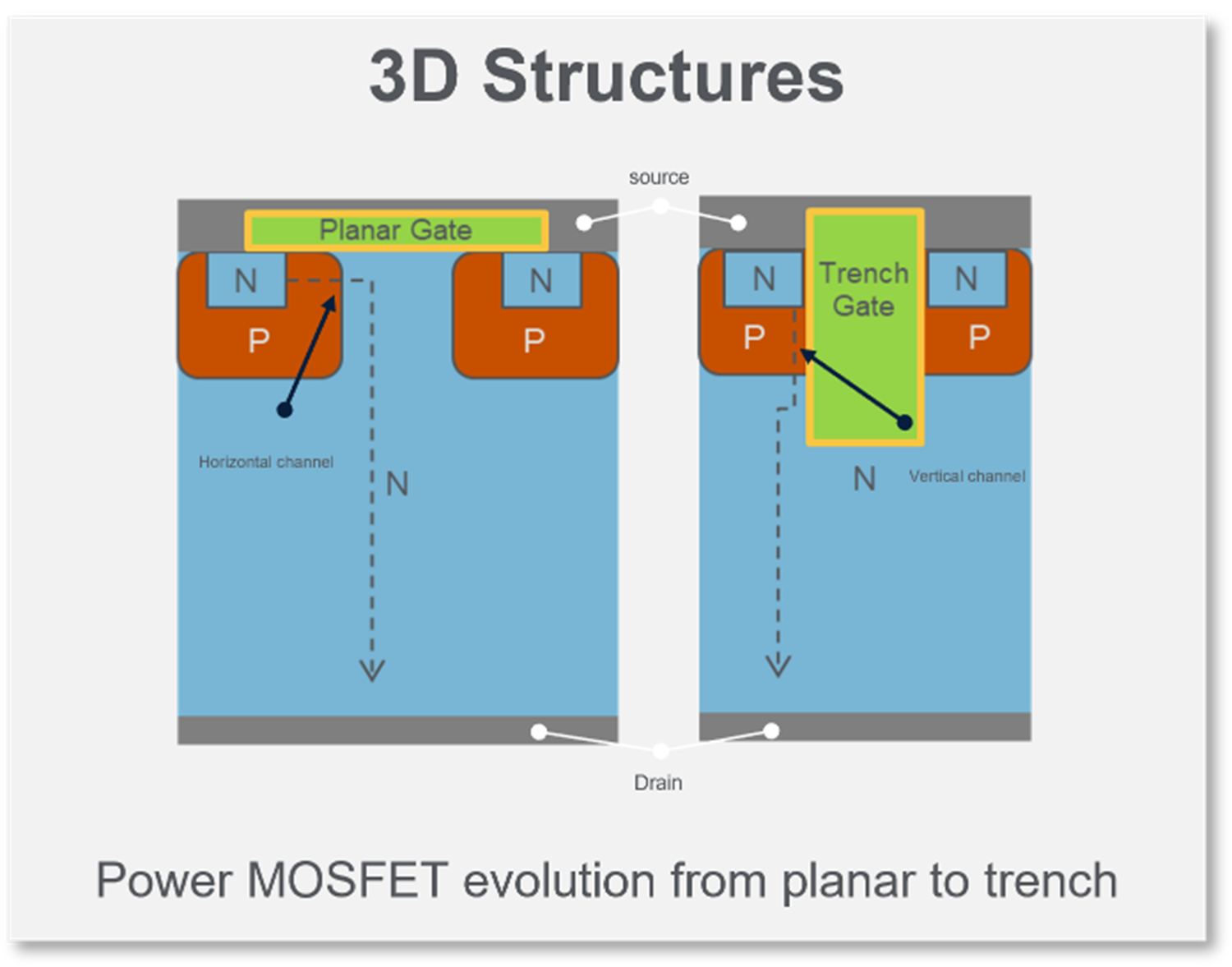
Beyond the wafer level, the power semiconductor device architecture roadmap is undergoing an evolution from planar MOSFETs to 3D trench MOSFETs and ultimately emerging “super junction” transistors. Each new 3D architecture brings a more vertical profile, resulting in taller and thinner structures with higher aspect ratios. These structures make it easier for buried defects to hide deep within trenches where they are more difficult to detect with traditional inspection techniques.
Harnessing High-Resolution eBeam for Defect Review
Chipmakers typically use two types of equipment to find and control manufacturing defects: optical inspection to detect potential defects on the wafer, followed by eBeam review, which provides much-higher resolution imaging capability to see and characterize defects in order to address their root causes. Optical inspection and eBeam review are complementary, and chipmakers typically combine the best characteristics of both tools to optimize yield and achieve faster time-to-market.
In today’s SiC fabs, chipmakers are primarily relying on optical inspection techniques for inline defect detection, without complementary high-resolution eBeam imaging characterization. Since the optical inspection’s image resolution is limited, a high portion of the tiny, buried SiC crystalline defects are misclassified in the fab process control flow, which can affect yield and device reliability.
To address this opportunity, Applied has developed the SEMVision™ G7C, a new defect review system designed specifically for compound semiconductor manufacturing. The SEMVision G7C offers high-resolution imaging with unique capabilities to better identify and classify SiC crystal irregularities and defects buried within 3D structures at high automation and productivity standards.
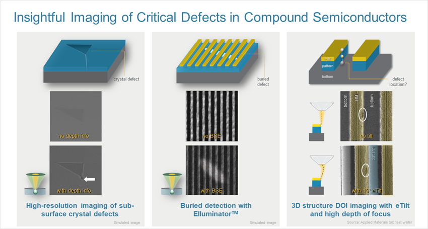
A key feature of the system is Applied’s Elluminator™ backscattered electron technology. It uses a wide-angle detector to collect more information from the high-energy electrons that penetrates the SiC wafer and carry information from the embedded defects at high resolution. The system allows chipmakers to see defects more clearly with greater depth and track their progress along the fab process steps. This technology also offers the ability to image buried defects in deep trench structures that otherwise would not be visible.
Another challenge with relying only on optical wafer inspection is that a defect may be visible from the top view, but it’s difficult to tell where the defect is located within the materials stack. For example, defects within a sacrificial hard mask layer are not a concern because the layer will be removed later in the fabrication process. But defects in the patterned device below the hard mask can cause reliability issues and potentially impact yield. The electron beam in the new SEMVision G7C can be electronically tilted by up to 10 degrees, giving fab engineers a sideview of the materials stack to better determine where the defects are located.
The SEMVision G7 family is widely recognized as the industry benchmark in high-resolution eBeam imaging. Applied is the global leader in eBeam technologies, with industry-leading market share and a long reputation for quality and productivity. We are excited to bring this unique, new set of capabilities to customers in the fast-growing market for SiC and other compound semiconductors.
Neta Shomrat
SEMVision Product Marketing, eBeam Defect Control Division

Neta Shomrat leads product marketing for Applied’s SEMVision product line, where she is responsible for driving the roadmap and strategy for advanced eBeam defect review technologies. A materials scientist with more than 10 years of experience in multidisciplinary research, technology development and commercialization, she holds a Ph.D. in energy and materials science from the Israel Institute of Technology (Technion).
Implant Innovation Enables the Compound Semiconductor Roadmap
AI may have taken center stage among the drivers for chip industry growth, but there is another global inflection fueling the semiconductor roadmap: the clean energy revolution. Featuring major structural shifts to renewable energy sources, smart grid technologies and electric vehicles, the star player in clean energy is the power semiconductor, which controls and converts electrical energy to supply power for a wide variety of electronic devices.
Understanding the Inflection in Wafer Fab Equipment Growth
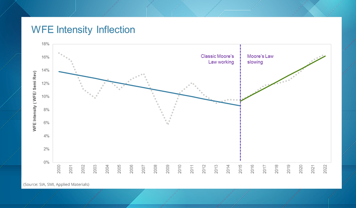
In my previous blog, I outlined a framework for why we at Applied Materials believe the wafer fab equipment (WFE) market can grow as fast or faster than the broader semiconductor industry.

Materials Engineering: The True Hero of Energy-Efficient Chip Performance
At imec’s 2024 ITF World conference, AMD CEO Lisa Su articulated a vision for a hundredfold improvement in compute power efficiency by the 2026-2027 timeframe, and said, “Driving performance gains over the next decade requires relentless focus on energy efficiency.” The emphasis on delivering energy-efficient compute extends well beyond AI servers to the PCs and smartphones we use every day.
