Products & Technologies
Products & Services
Contact
Back to Menu
Products & Services
Products & Technologies
Services
Resources
Contact
Posted
September 05, 2024

Stay updated on our content.
Implant Innovation Enables the Compound Semiconductor Roadmap
By Stephen Krause
September 5, 2024
AI may have taken center stage among the drivers for chip industry growth, but there is another global inflection fueling the semiconductor roadmap: the clean energy revolution. Featuring major structural shifts to renewable energy sources, smart grid technologies and electric vehicles, the star player in clean energy is the power semiconductor, which controls and converts electrical energy to supply power for a wide variety of electronic devices.
While power chips are not manufactured with the bleeding-edge process technologies behind the latest AI accelerators, there is still a tremendous amount of innovation needed to continue scaling power electronics for emerging applications. Many of these devices are built on silicon today, but there is a growing wave of interest in compound semiconductors such as silicon carbide (SiC), which have unique material properties that allow them to switch more efficiently and dissipate less power.
Because compound semiconductors have dramatically different properties than silicon, new manufacturing techniques and processing equipment are required to bring these promising technologies to high-volume production.
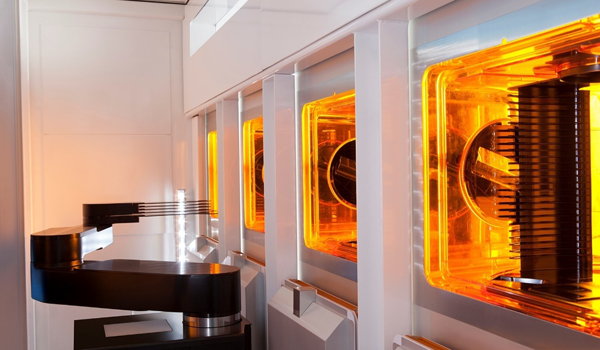
One of the key process technologies for SiC is ion implantation, or “implant” as it is more commonly known. Precisely injecting charged ions into a semiconductor crystal lattice creates the active region that controls the flow of current through the transistor. Applied Materials is the industry’s leading provider of implant technologies with systems designed for all key application segments, from high-current implanters for transistor source/drain development to high-energy implanters for very deep wells. Our implant products are built on common single-wafer, line-of-sight, triple-magnet beamline platforms that have been proven in production for decades, with an unmatched installed base of nearly 5,000 systems.
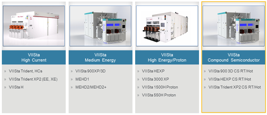
In recent years, we have extended our industry-leading VIISta platform to serve the growing SiC space. This allows us to leverage the platform’s maturity and scalability, applying years of learning to give SiC customers a performance edge in a production environment. The VIISta CS (Compound Semiconductor) product fleet uses a multi-tool strategy that delivers best-in-class device performance and yield as well as the lowest cost of ownership in high-volume manufacturing scenarios.
Harnessing High-Temperature Implant
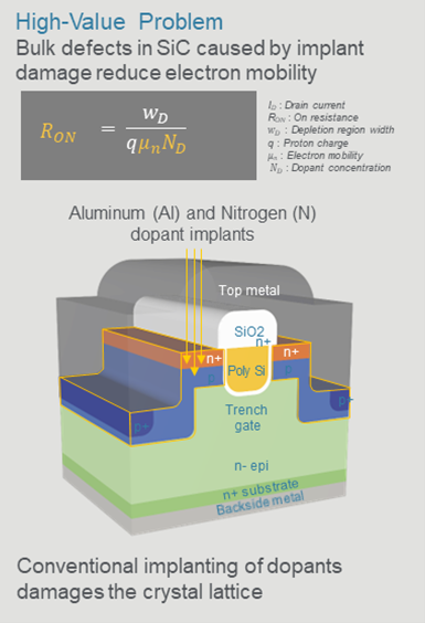
The efficiency of a SiC chip is governed largely by its “on resistance,” or how much energy it takes to flow current when the transistor is switched on. Lower on resistance equates to higher performance and lower power consumption. One way to reduce the on resistance is by increasing the mobility of electrons in the crystal lattice. However, implanting ions in SiC wafers and diffusing them in the material is much more challenging than in silicon wafers, which creates the need for more implant layers for graded implant profiles.
In 2021, Applied introduced the first member of the new CS fleet – the VIISta® 900 3D – to help overcome this challenge. This system leverages “hot implant” technology that uses 500-degree-Celsius temperature and medium-current energy to inject ions without severely disrupting the lattice, thereby maximizing electron mobility and dramatically reducing resistivity. This system has seen steady customer adoption with more than 3X growth in the installed base since introduction.
The VIISta 900 3D system is a great solution with a broad energy range, but we have also introduced systems that are optimized for more specific compound semiconductor applications. The VIISta Trident XP2 is a high-current system featuring an aluminum source that is much more productive at lower energies, while the VIISta HEXP system can achieve the highest energies to enable deeper ion implantation.
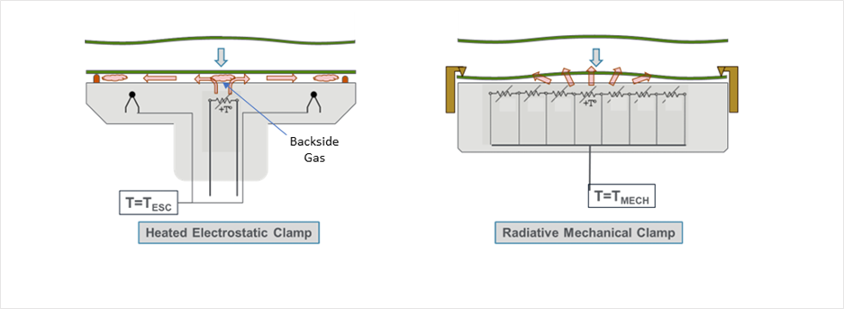
Each of these systems share one differentiating feature: Thermion™, the industry’s only high-temperature electrostatic chuck. While most industry solutions use mechanical clamps to hold the wafer in place, our approach combines targeted heating with backside gas to uniformly heat the wafer. In addition, electrostatic force helps maintain a flatter wafer profile. This not only minimizes damage during processing – a critical factor given the high cost of SiC wafers – but it also ensures greater control over the depth of implant from the particle beam.
An Evolving Roadmap
Just like the leading-edge logic roadmap has transitioned from 2D planar transistors to 3D FinFET and Gate-All-Around transistors, the power semiconductor roadmap is going through its own 3D evolution to enable continued scaling. As power chipmakers move from planar MOSFETs to trench MOSFETs and ultimately emerging “super junction” transistors, each new architecture requires more complex device design with higher implant intensity. This added complexity drives more implant requirements, including the ability to implant with higher productivity and better control of the implant angle.
There is currently a gap in our industry’s ability to enable this critical design transition. To meet the implant requirements of next-generation power semiconductors, chipmakers need a system with the broad energy range of the VIISta 900 3D, but with higher currents and the ability to deliver a greater dose of ions with each pass. As we continue to refine our product offerings, we are in the process of developing a new system that would complement Applied’s existing offerings to deliver a formidable solution to maximize output and minimize cost-of-ownership for chipmakers.
In addition to introducing new technologies, we have enabled our manufacturing footprint to meet unprecedented demand for our implant systems by expanding the manufacturing capacity at our facility in Gloucester, Massachusetts.
Thanks to the unmatched performance benefits of the VIISta CS platform, Applied is the implant provider of choice at multiple Tier 1 SiC manufacturing sites for both 150mm and 200mm wafers. And our new products are adding to the momentum of our broader implant business, which grew by more than 50 percent in 2023 to give Applied over 60 percent share of the total implant market1. We are well positioned to provide the materials engineering solutions our customers need to continue driving innovation in compound semiconductors.
Members of our technical team will be sharing more details at the upcoming International Conference on Ion Implantation Technology 2024 in Toyama, Japan from September 20-26. Applied is a platinum sponsor of the conference, where my colleague David Zou will deliver an invited talk about implant challenges for current and future generations of power electronics devices, including novel implant approaches that can improve power device performance, overall yield and meet the stringent reliability requirements of the automotive industry.
1 TechInsights 2023 WFE Market Share
Stephen Krause
General Manager, Managing Director, ICAPS & High Energy Implant Products
Stephen Krause leads the ICAPS & High Energy Implant Products group at Applied Materials, where he is responsible for business development and strategy, product roadmaps, engineering, applications execution, and global customer engagements. Stephen has more than 25 years of experience at Applied, joining the company in 1996 as a mechanical engineer. He has thirteen patents, a bachelor’s degree in mechanical engineering from Rensselaer Polytechnic Institute, and a master’s degree in mechanical engineering from Tufts University.
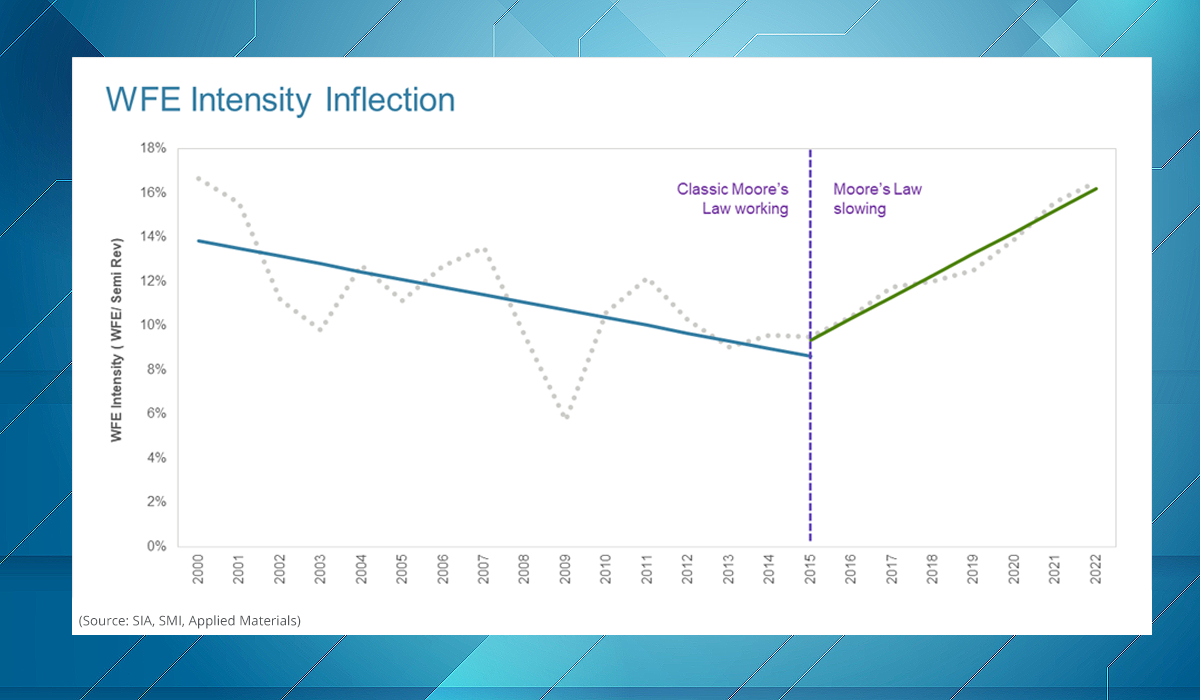
Understanding the Inflection in Wafer Fab Equipment Growth
In my previous blog, I outlined a framework for why we at Applied Materials believe the wafer fab equipment (WFE) market can grow as fast or faster than the broader semiconductor industry.
Materials Engineering: The True Hero of Energy-Efficient Chip Performance
At imec’s 2024 ITF World conference, AMD CEO Lisa Su articulated a vision for a hundredfold improvement in compute power efficiency by the 2026-2027 timeframe, and said, “Driving performance gains over the next decade requires relentless focus on energy efficiency.” The emphasis on delivering energy-efficient compute extends well beyond AI servers to the PCs and smartphones we use every day.
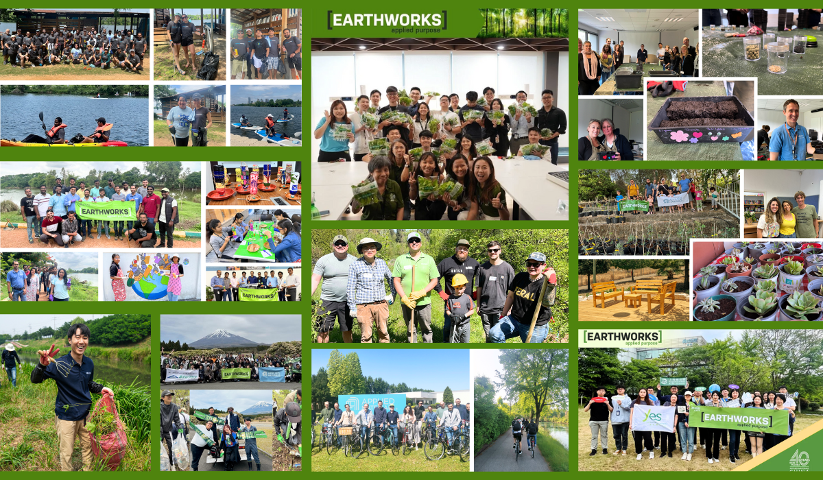
Applied Materials Employees Rally Together for Environmental Sustainability
At Applied Materials, we strive to Make Possible® a Better Future every day – and one of the ways we activate this vision is through our EarthWorks environmental campaign. Throughout the spring, Applied Materials employees from across the globe joined together to explore the natural world and inspire action for environmental sustainability.