Back to Menu
製品情報
AKT® eBeam Review
Advanced display technologies require an increasing number of process steps resulting in more and smaller contaminates, and new types of defects.
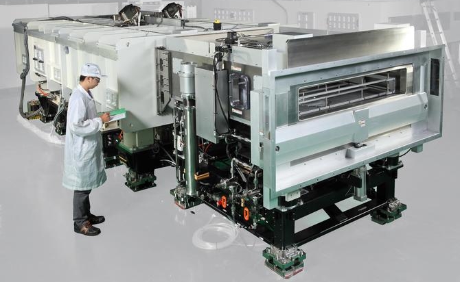
Current inline automated optical defect inspection tools for displays are not as effective as scanning electron microscopy (SEM) analysis in distinguishing killer from non-killer defects, or in determining systematic root causes of defects. Prior to the introduction of Applied’s eBeam Review (EBR) system, conducting SEM analysis on displays required breaking the glass substrate into pieces and examining each piece separately under a microscope. This is not only costly and time consuming, but also makes it nearly impossible to connect the defect behavior with final device performance. Applied solves these limitations by providing inline SEM review at the industry’s highest resolution and throughput without requiring the panel to be broken.

