Products & Technologies
Products & Services
Company
Contact
Back to Menu
Products & Services
Products & Technologies
Services
Resources
Company
Contact
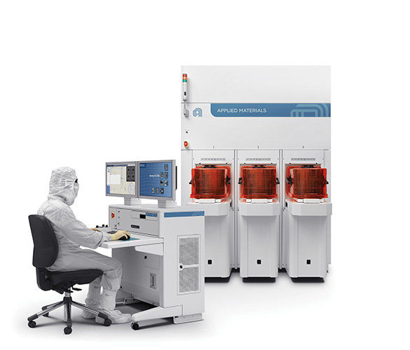
VeritySEM® 6D Critical Dimension (CD) Metrology
As the products we use and the world around us get smarter each year, there is an increasing demand for chips and the use of dielectric materials, which are great electrical insulators and energy storage elements… think capacitors and memory cells! A popular dielectric in the semiconductor field is glass for its lower electrical loss, better thermal stability, higher stiffness and transparency. Glass is growing in optical interconnects, where glass’s optical clarity makes it suitable for the transmission of light signals in many applications, including virtual and augmented reality (VR and AR), MEMS, CMOS image sensors, memory and logic, RF and power electronics, and fan-out wafer-level packaging.
Manufacturing dielectrics in high volume poses challenges for process control. Dielectric structures and films are susceptible to unwanted charging during the fabrication process, so wafers must be handled differently than silicon wafers. Dielectrics are fabricated on multiple wafer sizes with a wide range of thicknesses, opacity, conductivity… and may include a mix of 2D and 3D structures. Patterns typically vary between 0.1um to >100um in size and require extremely tight process variations that are critical for device performance. A CD-SEM (critical dimension scanning electron microscope) that is versatile in wafer handling and precision measurements can be tailored for dielectrics and address the varying degree of metrology and process control requirements.
As an extension of the popular VeritySEM 6i system that is used by most chipmakers worldwide, the Applied VeritySEM 6D CD metrology system enables advanced metrology and process control of dielectric materials, including glass and sapphire, as well as compound semiconductors and traditional silicon. The automatic wafer handling system self-adjusts to support 6’’, 8’’ and 12’’ wafer diameters of varying electrical and physical characteristics, such as wafer thickness and warpage. The VeritySEM 6D system also delivers high imaging resolution and detection efficiency to maximize throughput, while advanced automation and industry-leading fleet matching accuracy virtually eliminate the need for tool operators. Precision specifications enable the VeritySEM 6D system to make state-of-the-art 3D and high aspect ratio (HAR) pattern measurements required by many device structures, including vertical transistors in power devices.