Products & Technologies
Products & Services
Company
Contact
Back to Menu
Products & Services
Products & Technologies
Services
Resources
Company
Contact
Reveal Defect Analysis and Process Characterization
High performance failure analysis and process control are increasingly important capabilities for successful semiconductor chip manufacturing, especially as devices become more complex. In recent years, the use of exotic compound semiconductor substrates and thicker material stacks have grown. These material stacks contain many high-aspect-ratio 3D structures that require frequent processing and characterization. Manufacturing compound semiconductors poses additional challenges for process control, since devices are fabricated on different wafer sizes with a wide range of thicknesses, opacity, and conductivity.
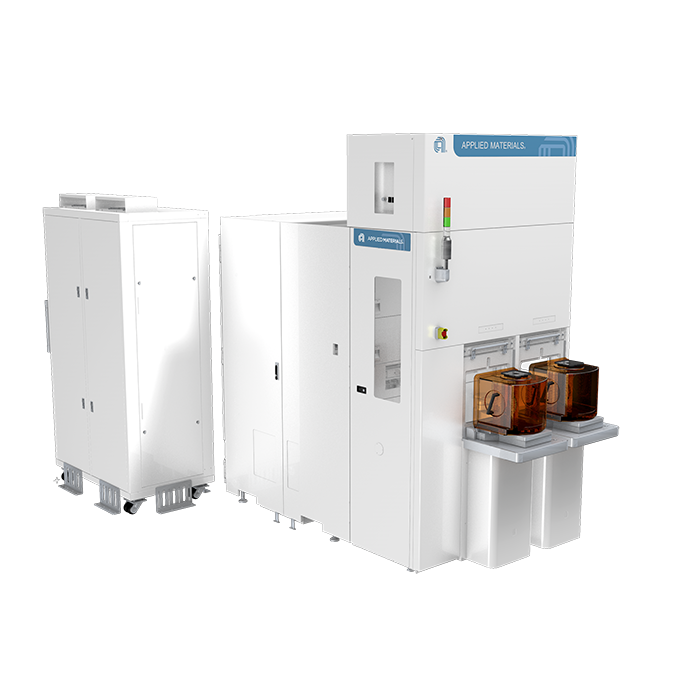
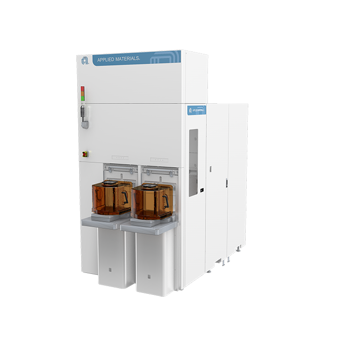
The Reveal™ system is an inline tool that supports standard semi and compound semi (conductive and nonconductive) substrates over a wide range of wafer sizes and thicknesses. The Reveal Ga is configured with dual SEM and gallium FIB columns; the Reveal Xe is equipped with dual SEM and xenon plasma FIB columns; the Reveal TR (tilt and rotation) is equipped with a single SEM column. For all configurations, the SEM column can be tilted at 0, 15 and 45 degrees, and the stage can be rotated. These tilt and rotation capabilities are essential for FIB cross-section imaging and detailed topography imaging of defects or specific structures characterization. The Reveal system provides multi-perspective images from several detectors. The top detector emphasizes the material contrast and side detectors emphasizes topography information. An energy filter is equipped for back scattered electron (BSE) imaging and an EDX detector provides material analysis. These inline capabilities are vital for successful process monitoring, defect control and root cause analysis (RCA), all while reducing cycle time.
The Reveal Ga and Reveal Xe provide inline recipe-based milling capabilities with high resolution SEM multi-perspective cross section images. The inline FIB milling capability and automatic SEM review reduce analysis to just a few hours versus the several days typically required by a TEM analysis from a failure analysis lab. Multiple wafer sites can be milled for uniformity analysis. This full-wafer capability enables a quick and deep understanding of entire structures and material composition needed to improve yield.
The Reveal Xe uses inert gas for milling which results in low contamination and high material removal rate. Reveal Xe can provide high-throughput plasma FIB milling needed for cross-section analysis, delayering, 3D reconstruction and 3D metrology. The system can reach 250µm depths. The Reveal Xe system is enhanced by multiple software components that collaborate to assume total command over failure and process analyses. A metrology server based on the well-adopted Verity® 7i CD-SEM engine enables critical dimension (CD) measurements to be overlayed on cross-section or top-down delayered images. Then, an embedded Data Cube application reconstructs 3D features using delayered images for complete 3D visualization of structures and cross-sections, complete with metrology. Enhanced defectivity analysis, including defect mapping and quantification, can also be performed across a three-dimensional landscape. These novel capabilities allow users to continuously monitor the correlation between design specifications and production results, which may reveal slow-moving process gaps that can negatively impact yield.
The Reveal family joins the SEMVision® family and a fleet of over 2,000 systems worldwide. SEMVision has been leading the inline defect review market since its introduction almost two decades ago.

- 1 / 3
- 2 / 3
- 3 / 3