Products & Technologies
Products & Services
Company
Contact
Products & Services
Products & Technologies
Services
Resources
Company
Contact
Enlight 3 Optical Inspection
Rising fab costs make the classic tradeoff between minimizing cost of ownership (CoO) and optimizing strategic control points along the manufacturing sequence much more difficult, leading to stricter limitations on the number of inspection steps. At the same time, the extremely small feature sizes of leading-edge transistors make yield-killing defects very challenging to differentiate from noise, where small variances can evolve into yield-killing defects when fabricating 3D structures and performing complex multi-patterning steps.
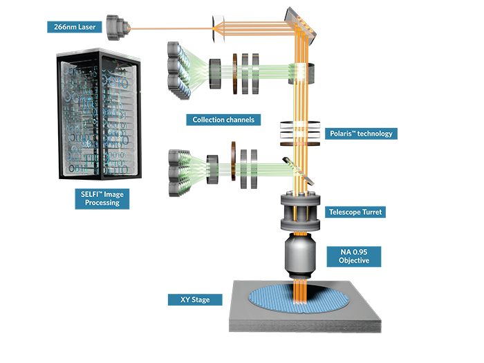
The Enlight™ 3 brightfield optical inspection system is part of Applied’s approach to reinventing process control so that chipmakers can achieve the required inspection sensitivity and frequency, collect more data, accelerate yields, and lower the cost per wafer. The system combines industry-leading optics with high resolution and advanced AI algorithms that capture more data per scan. Its unique architecture features the highest numerical aperture in the market to achieve a high-resolution scan and unique 3D polarization control that suppresses wafer noise. It also features simultaneous brightfield and greyfield detection channels, enabling a new generation of high-quality Big Data in production.
New signal enhancement, AI algorithms and throughput capabilities make the Enlight 3 our strongest optical inspection option. The Enlight 3 also covers a very large application space, from high-end brightfield to 30 wafers-per-hour (WPH) darkfield applications.
Chipmakers may lower inspection tool sensitivity to minimize nuisance detection, but this increases the risk of missing critical defects. To alleviate this challenge, Applied ExtractAI* uses big data from the Enlight 3 to help customers rapidly create fully classified noise-free maps during in-line monitoring.
The predictive capabilities of the Enlight 3 system, combined with Applied’s third generation ExtractAI technology, provides a real-time intelligent link between brightfield optical wafer inspection and our industry-leading eBeam review system, SEMVision™. This powerful trio produces adaptive AI-based pattern recognition that process engineers can harness to produce actionable insights about yield-killing defects or used by chipmakers to lower CoO, increase yield, accelerate development, speed time to revenue and increase profits over the life of a node.

Applied’s Enlight optical inspection, ExtractAI™ technology, and SEMVision eBeam review together deliver the most actionable data at the fastest rate to accelerate time to market of new process nodes.


- 1 / 3
- 2 / 3
- 3 / 3
*ExtractAI technology quickly and accurately distinguishes yield-killing defects from the millions of nuisance signals or “noise” generated by high-end optical scanners. ExtractAI technology is incredibly efficient; it characterizes all of the potential defects on the wafer map after reviewing only 0.001X of the samples. The result is an actionable map of classified defects that accelerates node development, ramp and yield.