Products & Technologies
Products & Services
Company
Contact
Back to Menu
Products & Services
Products & Technologies
Services
Resources
Company
Contact
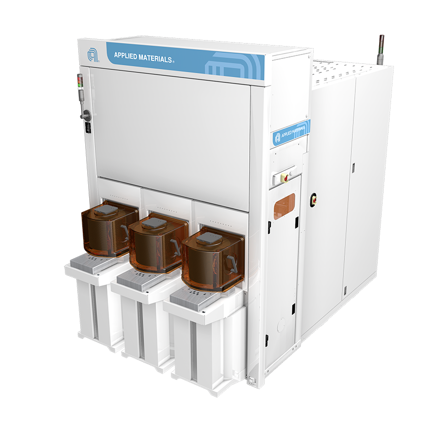
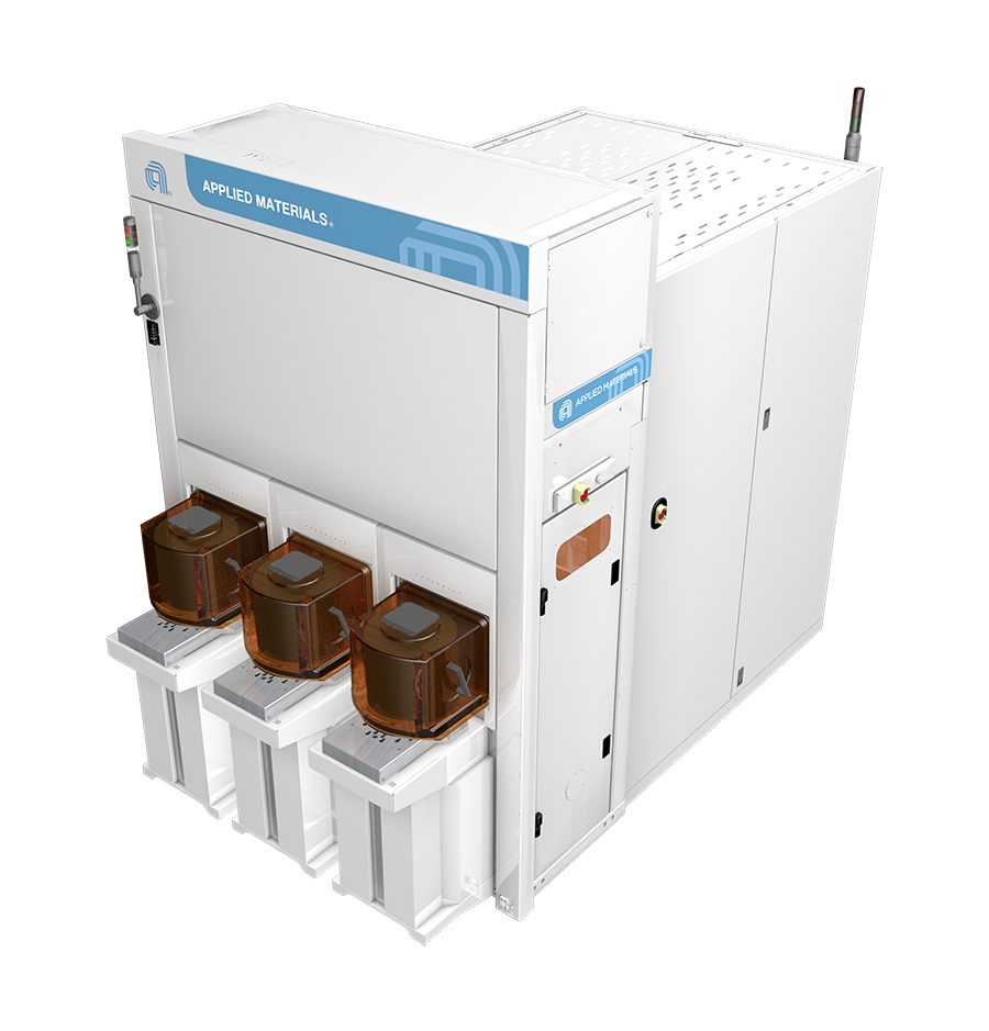
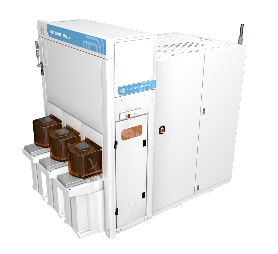
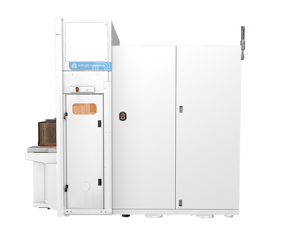
SEMVision G7 Defect Analysis
e-Beam defect review, classification, and analysis are vital to semiconductor fabrication as the means to monitor and control the quality of individual steps in the manufacturing sequence. The growth in chip production driven by advancements in automotive, IoT, RF, photonics, power and advanced packaging forces innovative process control to meet new industry standards and requirements. Innovation in device architectures and the introduction of new wafer types, such as compound semiconductors, call for constant enhancement of imaging capabilities to rapidly identify defects of interest. High-resolution images that are accurately classified enable reliable determination of root causes and are essential in establishing precise statistical process control, ultimately leading to accelerated production ramps and higher yields.
To meet these demands, the Applied SEMVision G7 family offers high resolution and advances in automatic defect review (ADR) and automatic defect classification (ADC). The family uses unique e-lluminator technology, an industry standard for back-scattered electron see-through imaging. Additionally, an electronic beam tilt and high depth of focus is used to detect defects in high aspect ratio and 3D structures. Fully automated recipe creation, defect detection, classification, and real-time analysis streamline the defect review process to maximize fab efficiency. Globally adopted Purity ADC capabilities ensure that defects of interest are represented in pareto charts, enabling corrective action implementations. Classifying defects using both SEM images and computer-aided design data produces precise location-based classification that facilitates faster, more accurate, root cause analysis and yield prediction. Covering the widest range of applications, including wafer-edge bevel and apex imaging, un-patterned wafer review and material analysis, the SEMVision G7 family supports defect review across all process steps.
The latest member of this family, the SEMVision G7C, is specifically designed to support emerging compound semiconductor markets and specialty devices through its automatic handling of different wafer types and thicknesses—SiC, GaN, GaAs and more. The system provides high-resolution imaging and in-depth information of surface and sub-surface crystallographic defects, addressing the unique performance and reliability characteristics of power and specialty devices.
- 1 / 4
- 2 / 4
- 3 / 4
- 4 / 4