
TABLE OF CONTENTS
A Letter from Ali Salehpour - Many Roads to Accelerate Time to Market
Boost Factory Productivity Faster With Applied SmartFactory™ Dispatching And Reporting
Breaking The Cycle—MtM Technologies Push Forward
In The Age of AI, Maydan Technology Center Evolves
E-Beam Review and CD Measurement Revolutionizes Display Yield Management
E-Beam Review and CD Measurement Revolutionizes Display Yield Management
By Kerry Cunningham
Fundamental changes are occurring in the display industry, driven by demands for higher-resolution screens and other capabilities for both mobile and TV applications.
To meet these demands, the display technology roadmap (table 1) calls for innovations in materials, processes and device technology. Critical requirements include smaller design rules and the adoption of a range of materials including copper (Cu), metal-oxides (MOx), low-temperature polysilicon (LTPS), organic LEDs (OLEDs) and even quantum dots (QDs). But new process- and materials-engineering expertise, as well as new yield-management strategies, are also required (table 2).
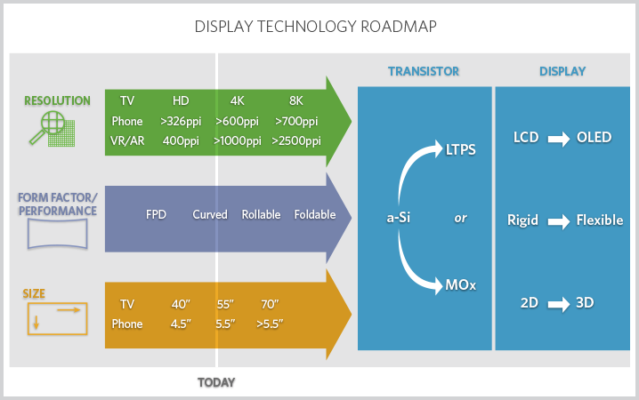
Table 1. Display technology roadmap. (Source: Applied Materials)
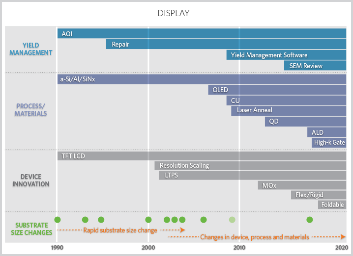
Table 2. Comparison of trends and factors impacting requirements for display yield management.
As TFTs in both OLED and LCD displays get smaller and screen sizes get larger, particles that were not problematic before may now become “killer” defects (figure 1). Equipment manufacturers therefore must find ways to reduce the number, size and density per unit area of particles when scaling to higher-resolution formats and to displays with smaller pixel sizes. Without such improvements in particle management, the resulting display yield losses will impact overall factory yields, productivity and profits.
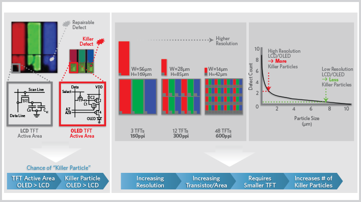
Figure 1. Killer defects are a critical and growing problem as displays move to OLED technology and to higher resolutions. New yield-management techniques brought over from the semiconductor industry are required to deal with them.
Yield excursions can be kept to a minimum by adopting new yield-management techniques from the semiconductor industry. This makes sense because the display industry is following a similar path to that of semiconductors, albeit some 20–30 years later.
Lessons From The Semiconductor Industry
From the early days of the semiconductor industry through the mid-1980s, there was rapid change in substrate sizes but relatively slower changes in devices, processes and materials. Since then, though, substrate sizes have changed less frequently but process and device changes—and complexity—have dramatically increased. It has been scaling or smaller design rules that have enabled high performance.
In terms of yield management, ever since device design rules approached ~1µm decades ago, the formerly best-known methods (BKMs) to monitor and control yield—optical inspection and review—have been inadequate. The resolution of optical tools reached its limit and the technical effort required to keep up with process requirements rose dramatically.
Electron beam (e-beam)-based inspection and review tools began to be used because they could easily accommodate ≤1µm design rules. They have since become a cornerstone of semiconductor yield management for defect review (DR) and measurement of critical dimensions (CDs).
It’s striking how similar the trend in display industry technology is to that of semiconductors. In the early years, display substrate scaling was the focus, with relatively incremental changes in the underlying processes and materials. Now though, smaller design rules and the adoption of new materials require not only new process- and materials-engineering expertise, but also new yield-management strategies. Thus the display industry can learn much from the semiconductor industry.
For example, the industry is now adopting e-beam technology for yield management using scanning electron microscopes (SEMs). Higher resolution is driving display CDs below 1µm, and today display is where semiconductor yield management was in the CD-SEM and SEM-review introduction stage in the 1980s (figures 2 and 3).
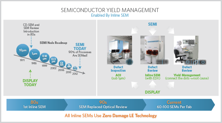
Figure 2. The display industry is beginning to develop more sophisticated yield-management techniques enabled by inline SEM-based defect review and CD measurement technologies.
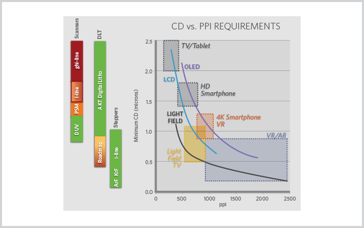
Figure 3. Higher numbers of pixels per inch and new multiple-view displays are driving display lithography.
Indeed with 1µm design rules, the display industry’s challenges are greater than those previously faced by the semiconductor industry. Today CD uniformity must be controlled on substrates that are ≥9 square meters large, while semiconductors were limited to 8-inch wafers.
A CD-SEM is a system for measuring the dimensions of the fine patterns formed on substrates such as glass panels. Mainly used in semiconductor manufacturing lines, it is now being adapted to meet panel-level fabrication requirements.
That is because the isolated and dense patterns used to build complex low-temperature polysilicon (LTPS) or MOx backplane TFTs require tighter lithography design rules. Below 1µm the degree of pattern alignment resulting from different process steps affects both process control and the number of induced defects per unit process. As pattern size is reduced, overlay (OL) discrepancies become larger and introduce critical defects.
Until now CD values have been measured using SEMs, and OL errors have been measured with optical tools. However as the display industry approaches <1µm design rules, e-beam critical dimension (ECD) measurement tools will replace optical technology for display requirements. They will also be used for better photolithography and etch process control (e.g., resist and pattern sidewall analysis) to achieve higher device performance (figure 4).

Figure 4. Photomicrographs illustrate the capability of ECD measurement tools to achieve 5–10nm resolution, which enables effective process control for display manufacturing at submicron design rules.
Inline inspection-based analytical techniques adapted from high-volume semiconductor manufacturing can help manufacturers of LTPS LCD and flexible OLED displays achieve optimum yields faster than traditional methods during production ramps. Using these techniques also allows manufacturers to capture millions of dollars in revenue and avoid costly yield excursions.
Minimize Killer Defects In Real Time
Applied Materials is always working on better ways to help customers solve their evolving metrology and inspection challenges.[1] To help display customers address these issues, Applied has introduced an analytical approach based on e-beam review (EBR) technology that will help LTPS display manufacturers minimize killer defects in real time when a process or tool is not performing to specifications (figure 5).
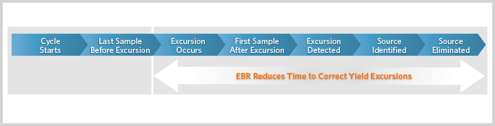
Figure 5. Yield excursion identification and correction cycle. (Source: AKT)
Applied’s EBR approach makes use of both SEM image analysis and SEM/energy-dispersive X-ray (EDX) tools, combined with large-scale display vacuum platforms. It can handle large-area glass substrates with no need to break the glass.
The idea is to isolate the most probable source of a defect (e.g., determine whether it arises from a CVD, PVD, etch, photolithography or other process step), then select the best sampling plan to isolate and monitor it. This approach enables proper preventive maintenance (PM) for process tools based on statistical process control (SPC) analysis of monitored defects, accelerating defect reduction.
Sample substrates are inspected after each process step. Automated optical inspection is used to generate a map of defects on these substrates. The substrates are then reviewed with the EBR SEM tool, and the results of that inspection are overlaid with the results of the optical inspection so that the EBR results can be analyzed to categorize the defects.
These tests should be repeated after each process step because the information gathered enables users to "work backward" from the defect to determine its root cause and get the problem fixed quickly. Not all defects are killer defects, and Applied’s EBR technology makes kill-ratio analysis possible. In this way, the tool or process step that is most likely to be the source of the problem can be more readily identified (figure 6). The resulting information is then fed into the fab’s yield-management system.
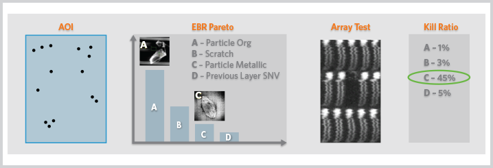
Figure 6. Kill-ratio analysis: Identifying which defects matter enables problems to be corrected quickly.
Applied’s EBR approach enables users to shave several months off the average 15-month fab ramp for LTPS displays. Assuming a factory output of 30,000 displays/month, a 3-month savings would be equivalent to $250M in added revenue.
Looking forward, EBR technology will become more important as the display industry moves farther along the path taken by the semiconductor industry. Today, semiconductor yield equipment represents about 12.8% of the total equipment spend per year. In display, however, yield equipment represents only 3% of the $17B display equipment market.
Given the increasing complexity of the transistors and other requirements for future displays, the market for display yield equipment should eventually approach the percentage levels of the semiconductor industry. This is essential to maintaining overall fab yield performance in the era of high-resolution screen requirements and complex device structures.
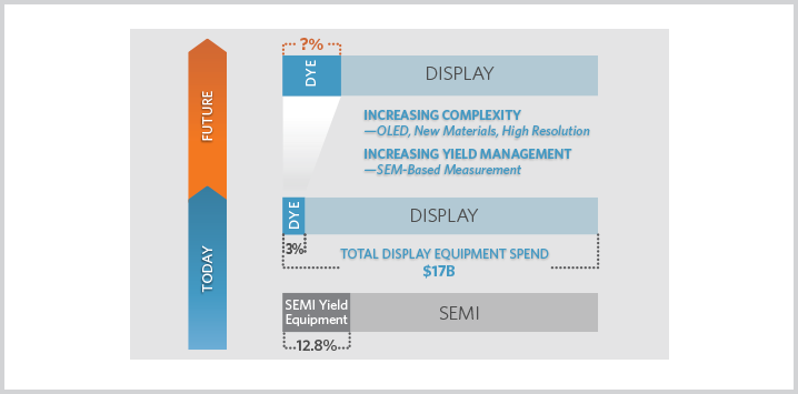
Figure 7. Percentage of capital expenditures for yield-enhancement equipment in the display and semiconductor equipment markets. (Source: Applied Materials)
For additional information, contact kerry_cunningham@amat.com
Kerry Cunningham is product marketing manager in the Display and Flexible Technology Group at Applied Materials.
[1] "New Metrology and Inspection Technologies Needed for More-than-Moore Markets," Nanochip Express, Fall 2018