Products & Technologies
Back to Menu
Products & Technologies
Services
Resources
Heterogeneous Integration
For decades, the semiconductor industry has relied on 2D shrinking and monolithic semiconductor integration which delivered simultaneous improvements in chip performance, power, area and cost. But as 2D scaling slows and becomes more expensive, chipmakers are increasingly moving in the direction of heterogeneous design and on-package integration of chiplets and devices to accelerate power, performance, area, cost and time to market (PPACt™).
While mainframes and PCs dominated the electronics industry, packaging served primarily to protect the silicon chip and connect to a printed circuit board (PCB). The main technologies used here were wire bonds. As mobile applications grew, packaging evolved to deliver functionality in a small form factor. Packaging bumps allow multiple connections between two parallel faces. Where necessary, fan-out repositions connection points, especially from the very tight pitch on a die to a more relaxed pitch on a PCB. Certain devices have seen the adoption of through-silicon vias (TSVs) which allow direct chip-to-chip connection. Each of these innovations increase packaging density and deliver higher speed and lower power consumption.
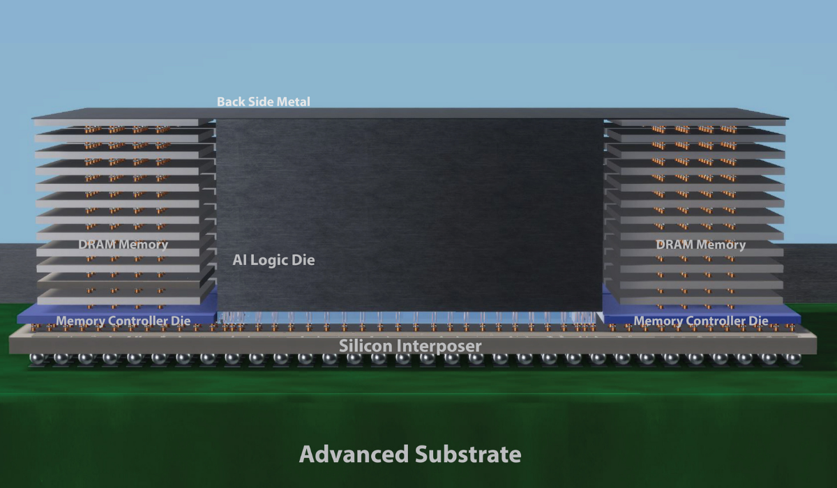
The desire to extract more system level performance at even lower power is leading designers to consider how to best integrate both chips and systems. Designers are finding it difficult to place the transistors they need for high-performance computing, machine learning and other AI processes on a single die. As an alternative approach, designers are using multi-die advanced packages that enable high-performance logic and memory in closer proximity, which reduces latency and power consumption. This approach called heterogeneous integration requires an extremely high density of short connections, orders of magnitude higher than offered by previous packaging technologies.
The move to heterogeneous integration needs two major breakthroughs:
- Hybrid bonding, whereby chips and wafers can be directly connected with copper.
- As more chiplets are integrated into a single package, packages need to be larger and more sophisticated. The industry is moving from silicon wafer substrates to larger advanced substrates.
Heterogeneous design is increasingly critical to meeting the PPACt roadmaps of the world’s leading semiconductor and systems companies. Applied Materials is helping to accelerate the trend through the unique breadth and depth of our industry-leading portfolio, along with industry partnerships and the world’s most advanced wafer-level packaging lab where our customers and partners innovate with us.

