Products & Technologies
Back to Menu
Products & Technologies
Services
Resources
TABLE OF CONTENTS
A Letter from Ali Salehpour - Many Roads to Accelerate Time to Market
Boost Factory Productivity Faster With Applied SmartFactory® Dispatching And Reporting
Breaking The Cycle—MtM Technologies Push Forward
In The Age of AI, Maydan Technology Center Evolves
E-Beam Review and CD Measurement Revolutionizes Display Yield Management
IN THE AGE OF AI, MAYDAN TECHNOLOGY CENTER EVOLVES
BY David Lammers
When the conversation turns to cooperative semiconductor R&D centers, Applied Materials’ Maydan Technology Center (MTC) in Silicon Valley may not immediately come to mind. But MTC is becoming a busy hub where semiconductor customers work cooperatively with Applied on an ever-widening variety of technical challenges, from logic and memory to emerging memories for AI, IoT and other areas.
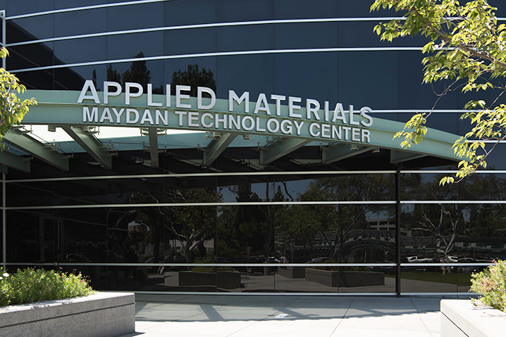
It wasn’t always this way. In the late 1990’s, Applied’s then-president, Dan Maydan, saw the need to develop a comprehensive solution and proving ground for customers facing the complex switch to copper interconnect processes. In response, in 1998 the company opened its Equipment and Process Integration Center (EPIC) facility in Santa Clara, California, near the Company’s headquarters. Subsequently, in March 2002, the MTC opened in its current, larger facility in nearby Sunnyvale, just as the industry transitioned from subtractive aluminum interconnects to Damascene copper.
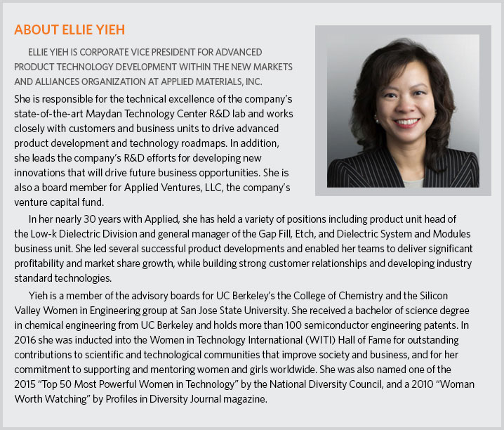
Ellie Yieh, Vice President of Advanced Product Technology Development, has managed MTC since 2013. Earlier in her career at Applied, she led the development of Black Diamond® low-k dielectric which was a key part of the overall copper solution.
"Early on, I worked very closely with the interconnect team at the EPIC facility to understand the impact of processing, before and after Black Diamond, on physical and electrical performance. MTC started with copper/low-k, offering customers a place where engineers could evaluate integrated solutions," she said. MTC’s work included gauging the impact of integration schemes on unit-process development and proving out the manufacturability before tools were shipped.
Materials Engineering Mandate
For a long time, Yieh said MTC focused mainly on unit processes and copper interconnects. Then, about five years ago, things began to change as Applied’s new CEO Gary Dickerson emphasized the need for forward-looking inflection-based innovation and a roadmap of new materials and more holistic solutions. The scope of MTC has since broadened and deepened considerably.
In mid-November, Applied Materials announced that it will develop the Materials Engineering Technology Accelerator (META Center) at the State University of New York Polytechnic Institute (SUNY Poly) campus in Albany. The META Center will expand Applied’s capabilities in advanced materials-based R&D, process technologies, device prototyping and pilot-scale production, shortening the timeline from Applied lab to customer fab.
Dickerson said the META Center "will extend the capabilities of our Maydan Technology Center to address the ecosystem’s growing need to accelerate innovation, from materials to systems."
As driving Moore’s Law becomes more challenging, Dickerson said "a new playbook is needed, which includes the development of entirely new chip architectures, new 3D structures within the chip, the integration of new exotic materials, new ways to shrink feature geometries -- including EUV lithography and self-aligned patterning -- and advanced packaging techniques to connect chips in new ways."
"Gary really believes in materials engineering innovations and the development of integrated materials solutions that speed progress as compared to sequential unit process innovation," Yieh said. “We needed to expand our capabilities to anticipate our customers’ future requirements.”
To fulfill this vision, MTC generated a surge of new solutions and test vehicles. The electrical results from these test vehicles provide direct validation of the materials-engineering solutions under study. The new and highly complex transition from copper to cobalt interconnects can only be explored and validated in this way. The widening variety of MTC test vehicles—ranging from simple MOSCAP to complex FinFET, 2-level metal, gate-all-around transistor and spin-torque magnetic RAM (STT-MRAM)—reflects the far-reaching set of opportunities being pursued at MTC.
"We have to be careful not to focus just on the most immediate problems," said Yieh. "We have to look out at least five years to make sure that Applied Materials is ready with the solutions our customers will need. We must give customers enough time so they don’t fall behind."
STT-MRAM Test Data
The magnetic memory effort started about five years ago with the goal of developing Applied’s STT-MRAM test vehicle, complete with electrical test data. This enabled MTC to validate multi-cathode PVD and ion-beam etch products and work with partners on a holistic integrated materials solution approach. The work led to joint papers with partners such as Qualcomm at major semiconductor conferences.
According to Yieh, "Customers started asking us, ‘How do you generate your electrical test data? What is your secret sauce?’ Customers listened to those papers and wanted to know how we created our material stack, how we did the etch, all of which helped position the equipment divisions to engage with customers eager to develop their own technology."
The positioning work paid off. One customer that is developing an MRAM solution bought multiple tools and associated integration services from Applied for pre-qualification.
"Last year sparked demand for Applied’s MRAM-related multi-cathode PVD products," Yieh said. "A big part of that is because business units were able to show our work here at MTC, demonstrating to customers that the equipment was meeting all of the requirements and was vetted through an integrated flow."

The development of an MRAM process within MTC led to an interesting agreement in November between Applied Materials and Fremont, California-based Spin Memory, Inc.[1] The companies will create an embedded MRAM solution that combines Applied’s MRAM capabilities—including its innovations in PVD and etch processes—with Spin Memory’s Precessional Spin Current™ (PSC™) structure, known as the Spin Polarizer.
The effort will give interested customers the choice to use this comprehensive embedded MRAM module in their own production flows. Spin Memory intends to make the solution commercially available next year, enabling customers to start producing MRAM-enabled products for both non-volatile (flash-like) and SRAM-replacement applications.
Separately, Spin Memory and semiconductor IP provider Arm Ltd. signed an agreement in which Spin will license its “Endurance Engine” design architecture to Arm so the latter can develop a new line of embedded MRAM design intellectual property.

Cobalt's Unique Challenges
Cobalt is another example of anticipating where technology is headed, as Applied Materials technologists saw that tungsten contacts and copper local interconnects could not be scaled much further without an excessive resistance penalty caused by scattering. MTC began evaluating cobalt’s unique challenges, including gap-fill, planarization, and metrology.
"We did a lot of studies on how to enable cobalt integration. It needs to adhere, it needs to be polish-able, it needs to gap fill, it needs to have no impact on electromigration or reliability. We did our work long before any customer came in and said they needed a cobalt solution for contacts. We already had it characterized, and that really accelerated time to market," Yieh said.
Yieh said that the MTC staff also cooperates in a number of ways with Applied Global Services (AGS) at the early development stage to make sure that new tools contribute to a fab’s productivity. For example, MTC has the Applied FSS advanced analytics technology, essential for the local and remote data-analysis capabilities that AGS is advancing.
Latest Tools an Advantage
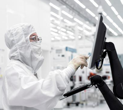
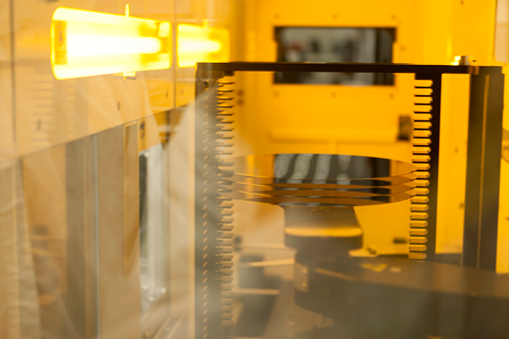
Applied’s breadth of tools is a competitive advantage. With over 300 pieces of equipment in 39,000 square feet of cleanroom, MTC is full and bustling with activity. All that state-of-the-art equipment attracts partners—including consortia and startups that often do not have the capital-equipment budgets for the most advanced tools, Yieh said.
"We have in-house mask design for our advanced test vehicles, as well as OPC [optical proximity correction] and multi-patterning capabilities, and we collaborate with outside partners for advanced lithography. Not only do we have the latest and greatest unit processing, we also have test vehicles to link them together. The breadth of our capabilities is a key differentiator," she said.

A Wide Range of Markets
Yieh has worked at Applied Materials for more than 25 years, much of that time directing the company’s product business units. When she came to MTC, she said, her enthusiasm doubled as she recognized the rich learning generated in MTC and the opportunities to build new solutions to close technology gaps.
And then the semiconductor industry itself took a turn, entering an accelerated period of growth, fueled by explosive amounts of data being generated, just as designers recognized that classic Moore’s Law scaling was not the only game in town. Technologists increasingly embraced a new agenda, one based not only on reducing transistor dimensions but more on introducing new materials and device structures. The challenges posed by the Internet of Things, emerging memories and AI pointed to huge new markets—and a redefinition of the industry. "Now more than ever, we are looking at new and emerging technologies that are taking place both at the most advanced and legacy nodes − those that are going to fuel growth for the company and our industry," she said. "There are a huge number of opportunities in front of us."

Putting Out A Welcome Mat To The Ecosystem
The Internet of Things is driving innovations in sensors, power management and data transfer, while data centers are pushing toward closer integration of memory and compute to overcome performance barriers. In addition to core customers, Yieh said many of the companies working in these new spaces are startups that need a place to prove out their ideas in silicon. They are attracted by MTC’s materials engineering capabilities and state-of-the-art technology. As a board member of Applied Ventures, LLC, the company’s venture capital arm, Yieh sees opportunities to work with startups. "We want to learn about new markets and have MTC enable their technology, accelerating time to market," she said.
"Some of these startups had no ideal place to do this kind of work," Yieh said. "Now we have multiple companies that want to come here and use MTC to validate their device performance. For instance, some companies may have concepts from a university that they now want to bring to MTC to confirm on 300mm wafers. This is a new way of collaboration for Applied, one that matches up well with our company’s mission to make possible the technology shaping the future. In addition to the challenges of shrinking and scaling, we can use our materials engineering expertise to help enable these innovators. Here at the MTC, we are in a position to make this happen faster," she said.
New Markets And Alliances Group
MTC’s role is central to the company’s New Markets and Alliances Group, announced this year and headed by Applied Senior Vice President Steve Ghanayem.[2] He too stressed a focus on addressing new market opportunities. "We want MTC to become an innovation engine not just for our existing customers, but for all those who want to build devices for new applications," Ghanayem said.
AI promises to be "the next big story for the foreseeable future," Yieh said. AI processors that adhere to the traditional Von Neumann architecture, in which the processor and memory are separated, suffer from the time and energy it takes to move data from memory to the processor. In-memory-compute is a promising alternative that dovetails with the research into new non-volatile memory types, such as resistive RAM, STT-MRAM and phase-change memory.
Avoiding Science Projects
Yieh said one of her biggest challenges is to help identify which jobs to tackle, and when to shelve an effort and move on to the next thing. "We look for inflections, identify new materials-enabled device performance and actively prioritize these opportunities. We have to look at the potential size of a market, and not just do science projects. How do we juggle all these prospects? There are huge opportunities out there. That’s why the industry is so exciting now, but in a very different way."

For additional information, contact nanochip_editor@amat.com
[1]https://www.businesswire.com/news/home/20181111005087/en/Spin-Memory-Tea...
[2]http://www.appliedmaterials.com/company/about/leadership/steve-ghanayem
