Products & Technologies

Products & Services
Company
Contact
Back to Menu
Products & Services
Products & Technologies
Services
Resources
Company
Contact
Posted
June 30, 2018

Stay updated on our content.
Why Materials Engineering Breakthroughs are Required for New AI Computing Architectures
Jun 30, 2018
This is the second installment of a two-part blog summarizing my presentation at the New Street Research Accelerated Computing conference hosted by Pierre Ferragu on May 30 in New York. I hope this summary will help everyone attending the upcoming #AIDesignForum being hosted by Applied Materials and SEMI on July 10 in San Francisco as a new track within SEMICON West.
In the first installment, I summarized how computing architecture requirements for AI workloads are different from what we became familiar with over the past couple of decades, in the form of traditional computing architectures such as x86 and ARM. In this post, I will also make the case that new AI computing architectures require materials engineering breakthroughs. I’ll give some examples of the types of breakthroughs we are referring to and describe one specific example in the area of new memory.
A Journey from Classic 2D Scaling to Architecture Innovation
In the PC and Mobile eras, which spanned more than 20 years, the industry was driven by “Classic 2D Scaling,” which refers to geometric transistor scaling as predicted by Moore’s Law in 1965. As transistor features got smaller, performance increased and power decreased consistent with Dennard’s Law. Higher transistor density also had the effect of lowering cost per transistor such that total chip cost decreased. During this period, we didn’t see a lot of architecture innovation, as a lot of focus was put on geometric scaling of a prevailing architecture, and this reinforced the rise of the x86 and ARM CPU architectures.
As you are probably aware, classic 2D scaling is no longer working as well as it used to. It has become very complex and very expensive, and the benefits it returns have been diminishing. So as we transition to the era of AI and IoT, a lot of emphasis is being placed on architecture changes to drive performance and power improvements. Architecture changes can drive a dramatically higher level of performance by fundamentally changing how data are processed. As you have probably seen with Google’s new TPUs, NVIDIA’s new GPUs and Microsoft’s Project Brainwave, the performance improvements relative to traditional CPUs are quoted in the order of magnitude and above range, e.g. 30x, 50x or even more. This is clearly a radically higher level of improvement versus what classic 2D scaling could provide, even in its best days. Architecture advances can be enabled by entirely new devices, or 3D techniques that can be used to extend existing logic and memory architectures, or even advanced packaging that brings diverse silicon together in new ways to perform specific functions.
In the sixth edition of their popular textbook published in December 2017, John Hennessy and David Patterson (widely regarded as the fathers of modern computer architecture) have meticulously summarized 40 years of processor performance data to make the case that three of the popular “laws” related to CPU performance progression have all effectively petered out. According to the reference, Dennard scaling ended in 2003, Amdahl’s Law reached its limits in around 2011, and Moore’s Law progress ended in around 2015. Our interpretation of their analysis is that the free ride of performance improvement from classic 2D scaling has effectively ended, and we now must work hard to combine architecture innovation and materials engineering breakthroughs to enable the performance improvements required for AI.
Applied’s Prabu Raja participated in a panel discussion with other industry luminaries earlier this year on this topic. If the definition and nomenclature of logic technology nodes interests you, you might enjoy a three-part blog I published recently.
Materials Engineering Breakthroughs
In the days of classic 2D scaling, materials engineering involved a limited set of materials such as silicon, silicon dioxide, silicon nitride and carbon. But these materials have already hit scaling limitations. In fact, we are effectively running out of materials on the periodic table that work well in isolation. We increasingly need to create unique variations, and this has given us 10 different types of silicon dioxide and eight types of silicon nitride, for example. In the new AI era, materials engineering increasingly involves creating new combinations of materials that work together as one system to enable specific properties. We call this Integrated Materials Systems.
As I discussed in the first blog post of this series, we believe there are three major architecture improvements needed for AI workloads: higher bandwidth memory, higher data parallelism and lower precision.
To achieve these improvements, we can draw upon materials engineering breakthroughs. For example, we can integrate new memory structures within existing logic devices. New materials can also enable entirely new memories such as Intel® 3D XPoint™ technology. We can use materials engineering to help self-align dense features such as the billions of vias present in GPUs. We can also use materials engineering to help vertically orient portions of the transistor for greater area density — as exemplified by Intel’s contact over active gate innovation. Materials engineering also plays a role in heterogeneous integration via advanced packaging: unique substrates, polymers and through silicon vias (TSV) can help enable denser packaging of a variety of separate chips.
Example: STT-MRAM
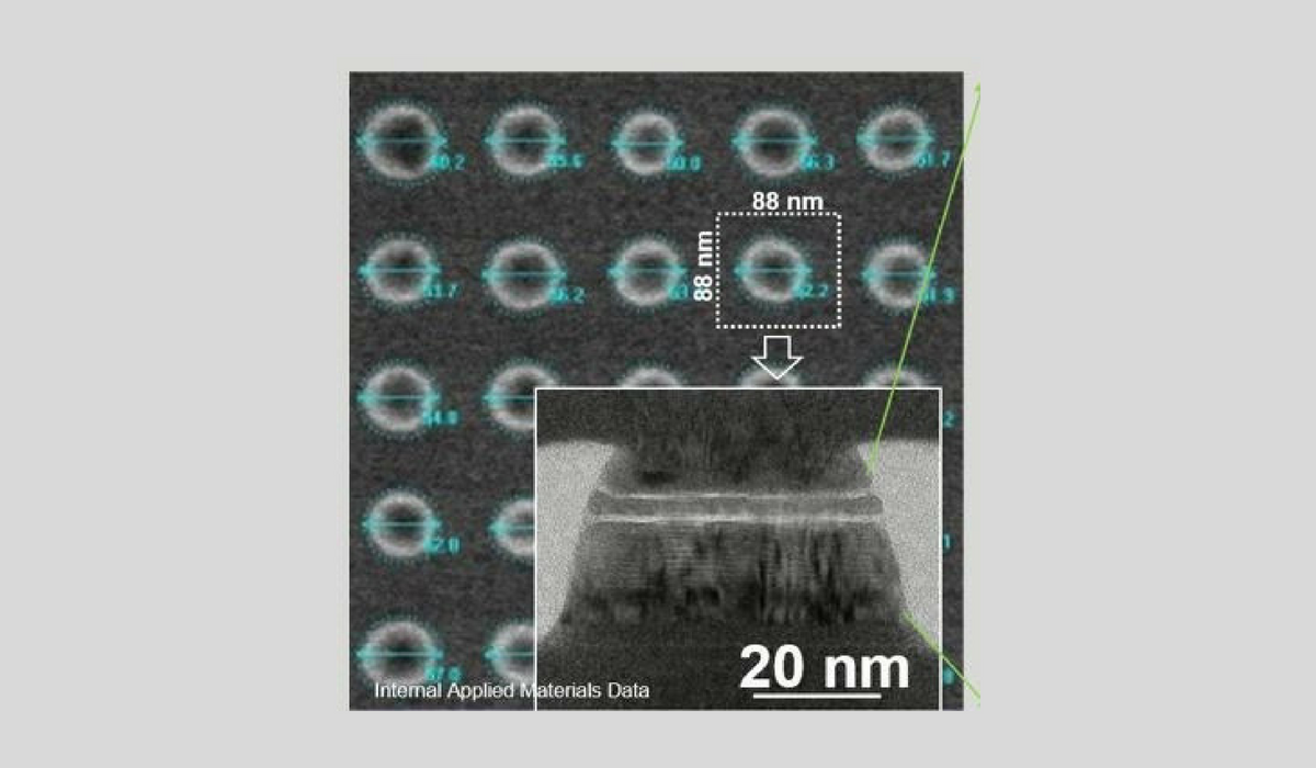
Here is an example of a materials engineering breakthrough used to enable a new type of memory. Below is a picture of an STT-MRAM array. The left side shows an array of memory cells, including a close-up of one of the memory cells. The right side shows how more than 15 materials have been stacked to help form the devices. The thickness of each of the films varies from 0.2nm to 2nm. By way of comparison, you may recall an innovation called High-K Metal Gate (HKMG) from about a decade ago; HKMG involved about six new materials, each about 1nm thick.
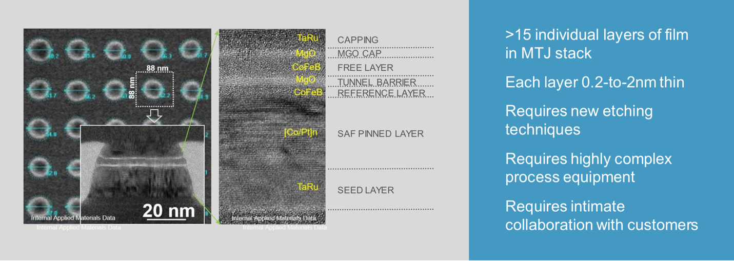
Source: Applied Materials
In the case of our Integrated Materials System for STT-MRAM, all of the processing has to be done in vacuum — in fact, in a much stronger vacuum measured at -9 to -10 TORR, compared to about -8 TORR vacuum for HKMG. (For reference, 1 TORR is equivalent to 1/760 of one atmosphere.) The interaction between layers of thin films of materials is called interface engineering, and this is what defines the properties of the resulting device. Producing the device requires carefully manipulating the materials using a variety of process technologies including deposition, etch and modification, all in an Integrated Materials System where the processing takes place in vacuum. Integrated Materials Solutions are what Applied Materials increasingly offers to help bring new architectural innovations into the industry. This capability is why our customers increasingly collaborate with us on advanced nodes and devices to prove such solutions and prepare them for high-volume manufacturing and commercial adoption.
Intimate Collaboration with Customers
At Applied Materials, we have been seeing a trend of deeper and earlier customer engagements, and we have been progressively investing more in our advanced R&D lab capabilities. Some of you may have visited our Maydan Technology Center (MTC) in Sunnyvale, CA. MTC is the most advanced 300mm R&D lab in the world. Applied has invested more than $300M in the facility over the past three years alone, and we are certainly not planning to stop there. Applied’s overall R&D investments have also increased to enable such materials engineering innovation. Another important part of how we fund innovation is through Applied Ventures, which currently has more than 30 active investments spanning a wide range of disciplines.
To summarize, I have two messages for you. First, AI workloads (i.e. machine learning, deep learning) require new ways to process data — we call this architecture innovation. Second, AI architectures require materials engineering breakthroughs. At Applied Materials, we are excited because we foresee AI driving a large growth opportunity for materials engineering. Join us at the #AIDesignForum to learn more, and bring your AI design challenges to Applied Materials — we look forward to collaborating with you!
Intel and 3D XPoint are trademarks of Intel Corporation or its subsidiaries in the U.S. and/or other countries.
Tags: artificial intelligence, AI, iot, Big Data, computing architecture, AI Design Forum
Sundeep Bajikar
Vice President and Head, Corporate Strategy and Marketing

Sundeep Bajikar is Vice President and Head, Corporate Strategy and Marketing at Applied Materials where he is responsible for shaping Applied’s strategies, including business and financial models related to the future of computing and Net Zero, in addition to tracking and analyzing Applied’s core business performance. He joined Applied in 2017 after spending ten years as a Senior Equity Research Analyst covering global technology stocks including Apple and Samsung Electronics, for Morgan Stanley and Jefferies. Previously he worked for a decade as researcher, ASIC Design Engineer, System Architect and Strategic Planning Manager at Intel Corporation.
He holds an MBA in finance from The Wharton School and M.S. degrees in electrical engineering and mechanical engineering from the University of Minnesota. He holds 13 U.S. and international patents with more than 30 additional patents pending. Sundeep is also author of a book titled, “Equity Research for the Technology Investor – Value Investing in Technology Stocks.”

Adding Sustainability to the Definition of Fab Performance
To enable a more sustainable semiconductor industry, new fabs must be designed to maximize output while reducing energy consumption and emissions. In this blog post, I examine Applied Materials’ efforts to drive fab sustainability through the process equipment we develop for chipmakers. It all starts with an evolution in the mindset of how these systems are designed.

Innovations in eBeam Metrology Enable a New Playbook for Patterning Control
The patterning challenges of today’s most advanced logic and memory chips can be solved with a new playbook that takes the industry from optical target-based approximation to actual, on-device measurements; limited statistical sampling to massive, across-wafer sampling; and single-layer patterning control to integrative multi-layer control. Applied’s new PROVision® 3E system is designed to enable this new playbook.

Breakthrough in Metrology Needed for Patterning Advanced Logic and Memory Chips
As the semiconductor industry increasingly moves from simple 2D chip designs to complex 3D designs based on multipatterning and EUV, patterning control has reached an inflection point. The optical overlay tools and techniques the semiconductor industry traditionally used to reduce errors are simply not precise enough for today’s leading-edge logic and memory chips.