Products & Technologies
Products & Services
Contact
Back to Menu
Products & Services
Products & Technologies
Services
Resources
Contact
Posted
May 18, 2018

Stay updated on our content.
The Role of CMP in Device Scaling
by Sameer Deshpande, Garlen Leung
May 18, 2018
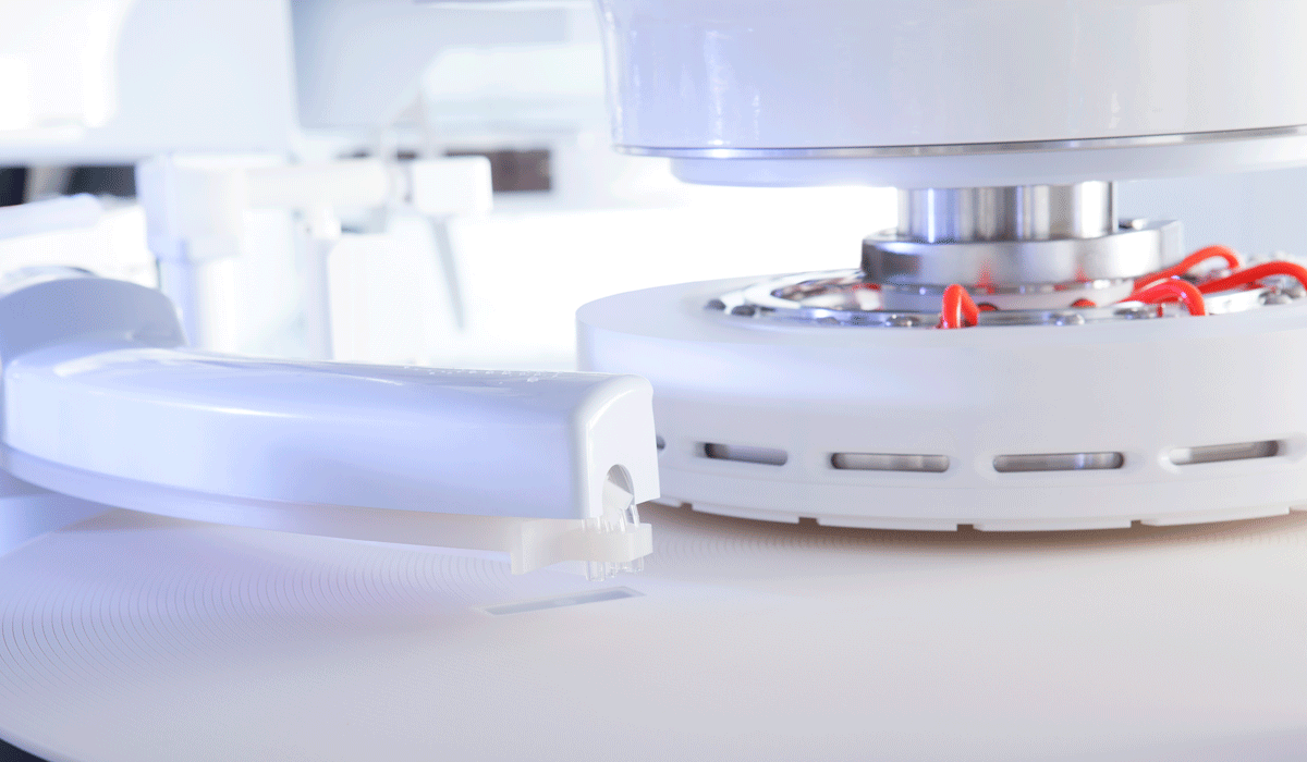
At the recent SPIE Advanced Lithography (AL) conference in San Jose, the firehose of information was, as usual, overwhelming. Every possible way to print and create the smallest features imaginable on a chip were discussed. So why would engineers who work on chemical mechanical planarization (CMP) technologies that make surfaces as flat as possible be at a lithography conference? Because CMP can facilitate chip designers’ drive for building ever-smaller features.
CMP has been an indispensable part of scaling for decades. Initially used to planarize multiple layers of silicon dioxide to form aluminum interconnects along with forming tungsten plugs, CMP applications have rapidly grown. CMP has been critical for enabling copper dual-damascene integration and, over the last decade, has supported transistor and device inflections. These include the replacement of metal gate where CMP was first used to create the gate, and FinFET transistors where additional CMP steps for the top gate and gate cap enable the transition from a 2D to 3D architecture.
Now it seems CMP may come to the rescue as the industry continues scaling, regardless of whether EUV will be ready for high-volume manufacturing (HVM) soon.
Historically, manufacturers scaled device designs geometrically using smaller wavelength lithography; but for the last decade, the industry has been stuck at 193nm immersion lithography. Many speakers at SPIE AL showed the great advances our industry has made for Moore’s Law scaling, but noted the corresponding offset for lithography-enabled scaling, which has stalled for the last few technology nodes. As Yan Borodovsky explained in his keynote address, while there is momentum and progress for EUV, there are many “gotchas” yet to be resolved for EUV in HVM, such as mask phase shifts and “stochastics” (a hot topic at the conference this year).[1]
So, what role can CMP play? As the industry sorts out EUV, we continue to move forward with materials-enabled methods for scaling. NAND flash makers took the leap by rotating the transistor 90 degrees to introduce a 3D architecture that continues NAND scaling without the need for EUV. CMP enables this change from 2D to 3D NAND with steps to manage the isolation for the taller structures and additional contact and via requirements.
Meanwhile, logic and DRAM makers have adopted alternative schemes to alleviate critical dimension (CD) shrink and pattern overlay requirements. Logic designs have converted layouts for critical layers from bi-directional to uni-directional layouts. This change allows multi-patterning schemes such as self-aligned double patterning (SADP) and self-aligned quadruple patterning (SAQP) to print the line patterns at CDs smaller than immersion lithography. However, after the lines are printed, they must be cut to create the necessary routing. Logic chipmakers are exploring an etch-fill-CMP scheme to achieve this. Recent images demonstrate where the gate lines are cut and how CMP can be used to polish back the gate cut fill.[2] This approach would be extendible to other 1D line prints moving forward.
At the SPIE AL conference, Imec explained the need to rely on design technology co-optimization (DTCO) where using “scaling boosters” enables improved power and performance for advanced logic. Imec further explained how a fully self-aligned gate contact (SAGC) can reduce standard cell track height by up to 15 percent.[3] This approach was also discussed at IEDM in December for the 10nm and below nodes [4], where it was described how dielectric caps can be added to the metal gate and the source/drain contact. To achieve this, a selective etch capability is needed as well as the ability to selectively CMP these cap materials.
What’s more interesting is that this multi-film scheme could potentially enable further scaling of vias in the back end of line. This could help address one of the biggest challenges to come — managing edge placement error (EPE) – another hot topic at the SPIE AL conference. These methods show that CMP can enable solutions for EPE in advanced nodes.
It is an exciting time for CMP as it becomes a vital enabling technology for the latest 3D inflections in NAND and logic, and for managing EPE. Future blog posts will continue to address challenges and advancements in CMP technology that can help keep the industry’s roadmap moving forward.
References
[1] Y. Borodovsky, “Moore’s Law at and beyond 5nm,” 2018 SPIE Advanced Lithography plenary presentation, Feb 26, 2018
[2] X. Wu et al, “Device for improving performance through gate cut last process,” 2017 U.S. Patent Application 15,590,459
[3] L. Mattii et al, "Efficient place and route enablement of 5-tracks standard-cells through EUV compatible N5 ruleset," Proc. SPIE 10588, Design-Process-Technology Co-optimization for Manufacturability XII, 1058803 (20 March 2018)
[4] C. Auth et al, “A 10nm high performance and low-power CMOS technology featuring 3rd generation FinFET transistors, Self-Aligned Quad Patterning, contact over active gate and cobalt local interconnects,” 2017 IEEE International Electron Devices Meeting (IEDM), San Francisco, CA, 2017, pp. 29.1.1-29.1.4.
Tags: chemical mechanical planarization, CMP, edge placement errors, EPE, SPIE Advanced Lithography, lithography
Sameer Deshpande
Global Product Manager

Sameer Deshpande is a Global Product Manager with the Chemical Mechanical Planarization (CMP) business unit in the Semiconductor Product Group (SPG) at Applied Materials. He is responsible for driving development teams to find solutions for CMP-specific challenges such as planarization efficiency, consumable performance stability and predictability, edge die yield improvements. He has authored over 20 publications and holds multiple U.S patents on various topics including surface engineered nanoscale transition metals and rare earth oxide ceramics, MEMs and CMP. Sameer holds a Ph.D. in Material Science & Engineering from the University of Central Florida.
Garlen Leung
Strategy and Marketing, Semiconductor Products Group

Garlen Leung works in Strategy and Marketing for the Semiconductor Products Group at Applied Materials. He received his bachelor of science and master of engineering degrees in materials science and engineering from the Massachusetts Institute of Technology and Cornell University, respectively.

Now is the Time for Flat Optics
For many centuries, optical technologies have utilized the same principles and components to bend and manipulate light. Now, another strategy to control light—metasurface optics or flat optics—is moving out of academic labs and heading toward commercial viability.

Seeing a Bright Future for Flat Optics
We are at the beginning of a new technological era for the field of optics. To accelerate the commercialization of Flat Optics, a larger collaborative effort is needed to scale the technology and deliver its full benefits to a wide range of applications.

Introducing Breakthroughs in Materials Engineering for DRAM Scaling
To help the industry meet global demand for more affordable, high-performance memory, Applied Materials today introduced solutions that support three levers of DRAM scaling.
![]()