Products & Technologies
Products & Services
Contact
Back to Menu
Products & Services
Products & Technologies
Services
Resources
Contact
Posted
March 11, 2021

Stay updated on our content.
Solving Big Problems in Defect Detection Requires Big Data
by Ortal Yesodi
Mar 11, 2021
Traditional Moore’s Law scaling is slowing dramatically. Yet, we need to move faster as an industry. If we can’t develop and ramp new semiconductor processes fast enough, and keep them yielding once they reach high-volume manufacturing, we face huge technical and financial obstacles to advancing the cloud, artificial intelligence (AI), the Internet of Things (IoT), the devices in our hands and more amazing things designers haven’t even thought of yet.
Part of being an engineer is believing that technology can solve any problem the world faces. Can it solve a problem at the very foundation of technology’s future? We think it can.
This is the second in a series of blogs examining challenges around defect detection and correction. The first blog outlined the problem of finding and correcting defects in the production processes that build advanced semiconductors. I explained that the industry’s legacy approach to defect detection is not working the way it used to because of three challenges.
The first challenge is keeping up with the soaring complexity of semiconductor process technologies and device structures. The prevailing industry approaches for optical defect detection were developed in a much simpler time that didn’t include extremely small line widths that turn tiny nuisance particles into yield-killing defects—along with the highly iterative processes used in 3D feature creation and multi-patterning wherein subtle variations multiply to create killer defects of unknown origin.
The second is rising cost. The number of process steps per wafer is skyrocketing, and so too is the cost of high-end optical inspection systems. While increasing complexity and process steps calls for more inspection points, the cost per scan is rising and tempting engineers to instead inspect less to help stay on budget.
But these are not the hardest inspection problem to overcome so that new technology nodes can move from R&D into high-volume manufacturing—and high revenue and profitability—faster. The third and toughest challenge is noise. Over time, the sensitivity of optical inspection systems has increased dramatically. For example, on a 12-inch wafer, they can produce a wafer map with a million potential defects. However, the vast majority of those signals are just nuisances, not yield-killing defects. But the sheer volume of signals can be overwhelming to fab engineers trying to debug a process, on time and on budget. As a result, they will often use filtering algorithms to get a more manageable data set to work with.
It may seem counterintuitive to pay all that money for increased sensitivity and then purposely filter the results, thereby reducing the amount of data being analyzed. The filtering essentially turns Big Data into little data. The smaller data set is more likely to miss yield-killing defects because the relative sizes of nuisance particles and real defects now overlap (see Figure 1). They look the same to the optical inspector, and the issue will only grow worse as features continue to shrink with the use of EUV lithography.
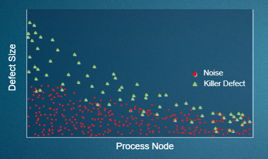
Figure 1: As process nodes advance, it becomes extremely difficult for optical inspection systems to distinguish between nuisance particles and killer defects.
Moreover, if the algorithms are not intelligent or adaptive enough, then a filtering scheme that worked fine on the original set of wafers may fail to detect changes in defectivity—and filter out killer defects that could have been detected. This false sense of security is dangerous and can be extraordinarily expensive.
The ideal solution, according to Applied’s researchers, would go in the opposite direction: move from little data to Big Data. Collect and analyze as much data as possible. Capture every yield data signature regardless of noise so nothing is missed. And find a breakthrough in technology that allows you to make inferences about particular signatures—both defects and noise—so that when you see and understand one signature, you have a chance of more quickly extrapolating that understanding across the entire wafer map. By rapidly classifying all the potential defects while also removing the noise, the ideal solution would give engineers an actionable wafer map of only the defects that require attention. No more guessing. No fear of what might be lurking in filtered data.
Today, the work of classifying potential defects is the job of scanning electron microscopes, like Applied’s industry leading SEMVision® eBeam review system which is widely used in fabs around the world. eBeam review systems have the extremely high pixel resolution needed to see and classify defects as well as distinguish defects from noise. However, it takes substantially much more time to scan wafers at such high resolution, so engineers typically use eBeam systems to review only small portions of wafers. This speed deficit makes a Big Data strategy impractical—unless we can find a way to somehow combine the speed of optical wafer inspection with the resolution of eBeam.
At Applied Materials, we have been talking for some time about how the industry is increasingly adopting a new playbook for driving improvements in chip performance, power, area/cost and time-to-market (PPACt). In order to modernize defect detection and correction in the AI Era, perhaps the industry also needs a new playbook for process control—one that improves the economics of high-end optical inspection and takes us from a world of little data to one of Big Data. Stay tuned for my next blog where I will describe what Applied is doing to make this world possible.
Tags: Process Control, inspection, Review, Defects, New Playbook, Big Data
Ortal Yesodi
Product Marketing Manager, Process Diagnostics and Control Group

Ortal Yesodi is a product marketing manager in the Process Diagnostics and Control group at Applied Materials. She joined Applied in 2013 and holds a bachelor’s degree in electrical and computer engineering from Ben Gurion University of the Negev.

Adding Sustainability to the Definition of Fab Performance
To enable a more sustainable semiconductor industry, new fabs must be designed to maximize output while reducing energy consumption and emissions. In this blog post, I examine Applied Materials’ efforts to drive fab sustainability through the process equipment we develop for chipmakers. It all starts with an evolution in the mindset of how these systems are designed.

Innovations in eBeam Metrology Enable a New Playbook for Patterning Control
The patterning challenges of today’s most advanced logic and memory chips can be solved with a new playbook that takes the industry from optical target-based approximation to actual, on-device measurements; limited statistical sampling to massive, across-wafer sampling; and single-layer patterning control to integrative multi-layer control. Applied’s new PROVision® 3E system is designed to enable this new playbook.

Breakthrough in Metrology Needed for Patterning Advanced Logic and Memory Chips
As the semiconductor industry increasingly moves from simple 2D chip designs to complex 3D designs based on multipatterning and EUV, patterning control has reached an inflection point. The optical overlay tools and techniques the semiconductor industry traditionally used to reduce errors are simply not precise enough for today’s leading-edge logic and memory chips.