Products & Technologies
Products & Services
Company
Contact
Back to Menu
Products & Services
Products & Technologies
Services
Resources
Company
Contact
Posted
February 26, 2025

Stay updated on our content.
Semiconductor R&D Leaders Share Vision for Accelerating Advanced Packaging
By Terry Lee
February 26, 2025
One of the primary hurdles to unlocking next-generation AI is the energy-efficient performance of chips. Advanced packaging technologies such as 2.5D and 3D integration are at the forefront of this effort. However, the path from innovation to commercialization is highly complex, and it requires a tremendous expansion in workforce. Industry-wide collaboration has never been more crucial.
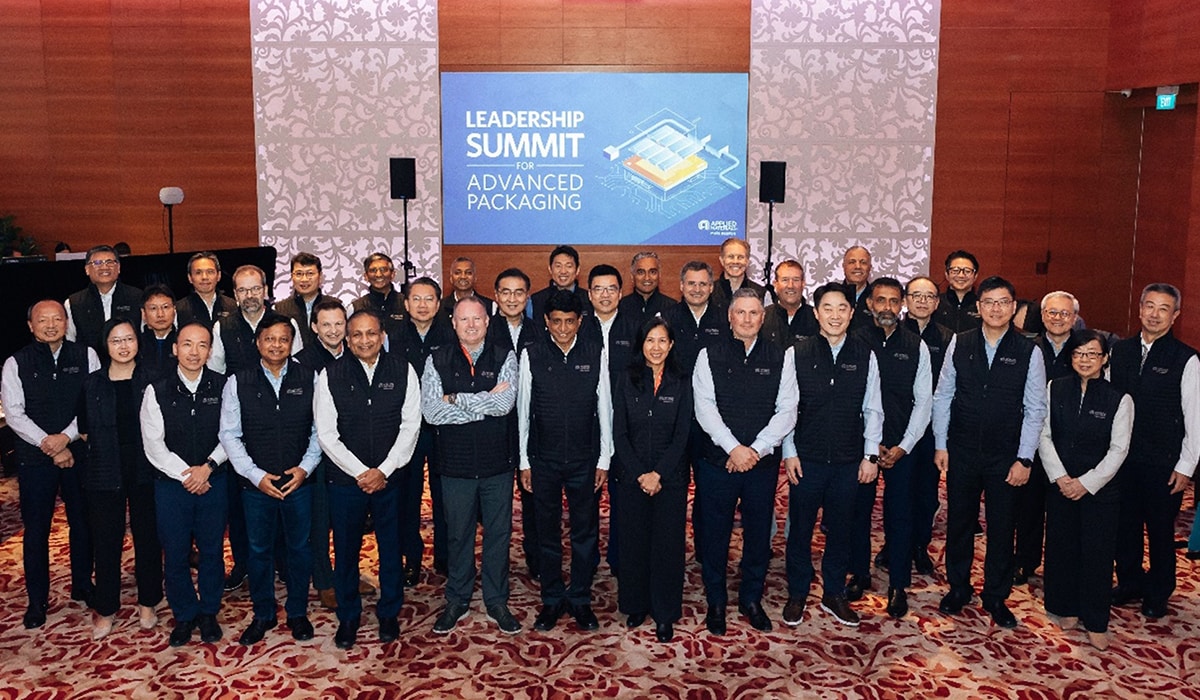
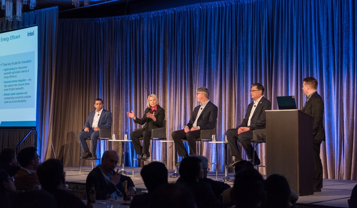
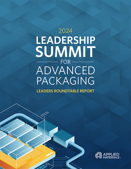 To address the challenges and opportunities of advanced packaging, Applied Materials hosted the inaugural Leadership Summit for Advanced Packaging as part of our EPIC Advanced Packaging announcement in Singapore. The cornerstone of the summit was our Leaders Roundtable, where more than 30 industry pioneers tackled two key topics: technology grand challenges, and building talent and capacity. Today, I am excited to share our report, detailing their key insights.
Attendees spanned the entire advanced packaging ecosystem, drawing leaders from chipmakers and system designers to equipment suppliers and OSATs. In a wide-ranging discussion facilitated by advanced packaging executives from AMD and TSMC, summit participants echoed the need for deeper collaboration, highlighting the potential of EPIC Advanced Packaging to help galvanize the industry.
Below are a few of the key themes that emerged from the sessions on challenges in both technology and talent.
Technology Grand Challenges:
Today’s most capable AI chips are enabled by multiple advanced packaging technologies, such as micro-bumps, through-silicon vias (TSVs) and silicon interposers. The next generation of chips will be built using advanced packaging techniques that require even more complex integration pathways. Some key building blocks discussed were:
- Hybrid bonding was highlighted by multiple participants as a critical building block for driving higher density connections. An emerging challenge is the need for extremely tight process control to manage particles that can cause defects, similar to front-end wafer processing fabs.
- Photonics promises significant improvement in energy-efficient performance, but more investment is needed to demonstrate the feasibility of high-density optical interconnects and to examine tradeoffs with conventional interconnects.
- The unique nature of glass substrates requires new approaches to inspection, metrology, handling, processing and forming interconnects.
- There is a growing need for thermal management techniques that focus on reducing heat generation, incorporating lower resistance interconnects in packages, and removing the waste heat produced in a packaged system.
- Several participants called for bridging the divide between front-end and back-end manufacturing processes, emphasizing the need for back-end manufacturing to incorporate learnings from the front-end – where the industry has converged on a common roadmap of key technology inflections.
Building Talent and Capacity:
The industry is facing a significant talent gap, with some estimating the need to recruit one million additional skilled workers over the next decade. This gap is driven by an insufficient number of graduates, an aging workforce, and a lack of appeal among potential candidates. Some recommendations from the summit include:
- Heterogeneous integration is not just about integrating technology components, but also about integrating people with different expertise – placing an emphasis on the need for a new kind of system-level thinking.
- Engineering curricula should reflect the increasingly interdisciplinary nature of advanced packaging.
- Many leaders called for innovative strategies to attract young talent, often drawing inspiration from the software industry. They stressed the need to improve the brand of the advanced packaging industry, leveraging creative tactics to improve the attractiveness of working in cleanroom environments.
- To the next generation of talent, doing meaningful work can be just as important as compensation and perks. To address this, the industry could better showcase its role in enabling solutions to the climate crisis while it focuses on creating more sustainable manufacturing processes.
- The industry should facilitate educational programs for young girls and women and ensure they can see role models in the semiconductor industry.
My key takeaway from the discussion is that we must innovate how we innovate. Industry-wide, global collaboration is essential to accelerating innovation in packaging technologies, closing the gap between the lab and the fab, and preparing a skilled workforce to meet the needs of this new era of energy-efficient computing. In the following video, several summit participants highlight the clear need for increased collaboration across the ecosystem, as well as earlier engagement with all parts of the value chain. To access more interviews with summit participants, please visit: 2024 Leadership Summit for Advanced Packaging.
The recommendations from the inaugural Leadership Summit for Advanced Packaging will help us enhance the vision and implementation of EPIC Advanced Packaging, and we plan to continue the series with our next roundtable planned for later in 2025. We look forward to working with our partners to address this need by driving co-innovation and changing the way foundational packaging technologies are developed and commercialized.
Terry Lee
Vice President and General Manager, Heterogeneous Integration

Terry Lee is the General Manager for the Heterogeneous Integration Business Unit. He is responsible for building and growing the advanced packaging business for Applied Materials. Previously, he worked in Etch, Dielectric Deposition, Chemical Mechanical Planarization and Plating Business Units. Before joining Applied Materials, he held executive positions in Business Development and Finance in the capital equipment sector. Mr. Lee earned a Bachelor of Science degree in Chemical Engineering from UC Berkeley and holds patents in CVD, CMP and Etch
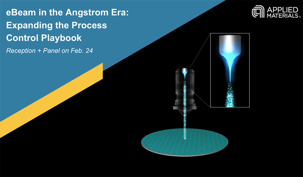
Expert Panel To Explore Advances in eBeam Technology
What’s New: Alongside the 2025 SPIE Advanced Lithography + Patterning conference in San Jose, CA, Applied Materials will bring together a panel of experts from across the semiconductor ecosystem to explore how chipmakers are increasingly using electron beam (eBeam) technology to continue pushing chip scaling to its limits. The discussion – featuring experts from IBM, imec, Intel and Samsung – will highlight emerging challenges in the “angstrom era” of chipmaking.
Advanced Packaging Enters a New Dimension
For more than a decade, Applied Materials has hosted a technical program alongside the IEEE International Electron Devices Meeting (IEDM) – the premier conference on leading-edge semiconductor technology. For this year’s program, we brought together some of the industry’s brightest minds to discuss the future of chip packaging in the AI era.

Celebrating 30 Years of Display Innovation
This month, Applied celebrated 30 years of innovation in display equipment. We have a long heritage of leveraging technologies developed for semiconductor manufacturing to help drive key display inflections, and we are well positioned to lead again in the next major inflection, which is bringing the superior OLED display technology found in high-end smartphones to millions more devices, ranging from AR/VR headsets to tablets, PCs and TVs.