Products & Technologies
Back to Menu
Products & Technologies
Services
Resources
Posted
July 16, 2024

Stay updated on our content.
The Race for AI Leadership is Fueled by Materials Engineering

By Kevin Moraes
July 16, 2024
At Applied Materials, we believe AI is the single biggest inflection of our lifetimes. However, the compute power required to support the growth of AI is driving energy consumption to new levels. Power is becoming a much more important variable, and we expect the demand for more power-efficient solutions to intensify. To achieve the full potential of AI, we must limit the growth in energy required to train new AI models.
At our SEMICON West Technology Breakfast in San Francisco, Applied executives and semiconductor device experts discussed the increasing role of materials engineering in enabling chipmaker roadmaps in logic, DRAM, high-bandwidth memory (HBM) and advanced packaging, all of which are critical to improving chip performance-per-watt. We were joined by AMD’s Mark Fuselier, Senior Vice President of Technology and Product Engineering, who explained the company’s computing technology vision and what’s needed from the equipment industry to support more energy-efficient AI.
Chip Architecture Inflections Are Becoming 3D
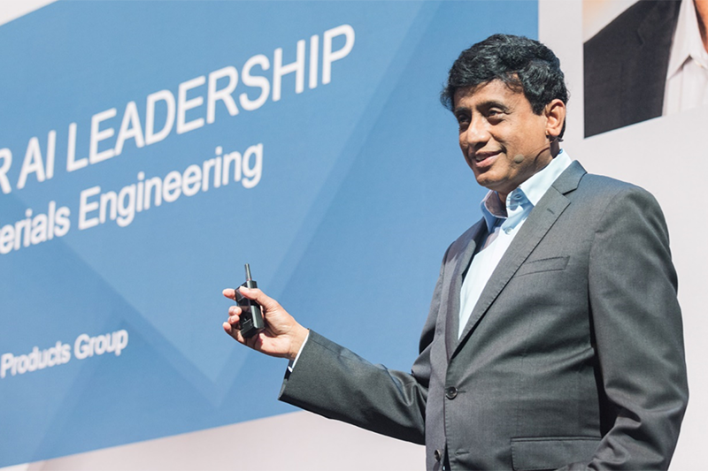
Prabu Raja, President of Applied’s Semiconductor Products Group, described the quest for more energy-efficient compute as “the race of a lifetime.” This race is driving the chipmaking industry to urgently deliver new innovations in transistors, frontside and backside wiring, and advanced packaging.
Prabu noted that traditional 2D scaling of devices no longer suffices. To deliver improved performance and lower power, all devices are becoming 3D. The industry is well on its way to adopting the Gate-All-Around (GAA) transistor architecture and advanced 3D packaging technologies such as hybrid bonding. Other technologies like Backside Power Delivery (BPD) and a next-generation DRAM vertical transistor will see adoption in the coming years.
These new 3D device architectures come with increasing process complexity, and Applied is addressing these challenges with its broad and connected portfolio, new collaboration models and an expanded innovation pipeline.

Prabu Raja, President of the Semiconductor Products Group at Applied Materials
Prabu gave an example of the increasing complexity using the GAA transistor, where the space between the nanosheets for the metal gate is only about 10nm. Advanced materials engineering technology is required to deposit more than five different materials in that extremely tiny area with angstrom-level precision at industrial scale. “Imagine you have to replicate 10 trillion transistors on a wafer. If you’re going to run a hundred thousand wafer starts per month, you have to replicate this day in and day out. That’s the complexity we are talking about,” said Prabu. Addressing this complexity requires new materials and technologies, as well as new combinations of process steps, which is driving an increased need for co-optimized and integrated solutions.
A Call to Action for the Equipment Industry
Following Prabu was Mark Fuselier, who described AMD’s efforts to improve the performance-per-watt of its products. The results thus far have been impressive. Mark explained how AMD has been able to reduce the energy per operation of its accelerator chip family by about 70 percent over three generations through very tight optimization of architecture and design, combined with low-power process technology as well as extreme focus on advanced packaging. While that’s significant, Mark indicated that AMD would like to further accelerate energy reduction.

Mark Fuselier, SVP of Technology and Product Engineering at AMD
Mark issued a call to action for increased innovation in thermal management, increasing the on-package power envelope, and tightly integrating memory and compute at both the package and system level – leveraging advanced packaging and optics to deliver solutions in an energy-efficient way.
Materials Engineering is the Foundation
Mark’s call to action set the stage for Mukund Srinivasan, Vice President and General Manager of Applied’s Integrated Materials Solution™ (IMS™) Group. Dedicated IMS teams work with Applied’s leading logic and memory customers to develop the next generations of technology through co-optimized and integrated solutions. Mukund highlighted how these teams work closely with all of our product groups to connect our technologies to best help our customers achieve their roadmap objectives.
Much of this work happens at Applied’s major R&D centers, including the Maydan Technology Center in Sunnyvale, the META center in New York, and our Advanced Packaging Development Center in Singapore.

Mukund Srinivasan, VP and GM of the Integrated Materials Solution (IMS) Group at Applied Materials
Looking ahead, Mukund explained how Applied’s EPIC Platform will include the industry’s largest and most advanced center for collaborative semiconductor process technology and manufacturing equipment R&D. It will give chipmakers early access to next-generation technologies and tools – months or even years before Applied can install them at customers’ R&D facilities – to accelerate high-velocity innovation and commercialization of foundational chip technologies.
Following his presentation, Mukund convened several of Applied’s technology experts who discussed the materials engineering roadmaps for logic, DRAM, HBM and advanced packaging.
Mehul Naik, Master and Vice President of Technology in the Semiconductor Products Group, described two critical areas of the logic roadmap: transistors and interconnect wiring. He showcased the materials engineering capabilities needed to deliver next-generation GAA transistors, while highlighting how more transistors on a chip translates to narrower wiring. Without interconnect innovations, narrower wires lead to reduced performance and increased power consumption – the opposite of what we need for AI.
Mehul described Applied’s comprehensive role in interconnect technology. He highlighted two innovations that Applied announced during SEMICON West that will help extend copper wiring to the 2nm node and beyond. One is Applied’s new enhanced Black Diamond™ material, a “low-κ” dielectric that insulates wires from each other. It reduces the minimum κ-value to enable scaling to 2nm and below, while offering increased mechanical strength which is becoming critical as chipmakers and systems companies take 3D logic and memory stacking to new heights.
The second innovation reduces wiring resistance. For the first time in the industry, Ruthenium and Cobalt have been combined to form a binary liner that is 33-percent thinner than its predecessor, for up to 25-percent lower electrical line resistance at the 2nm node. To achieve this materials engineering breakthrough, the new Applied Endura™ Copper Barrier Seed IMS™ with Volta™ Ruthenium CVD combines six different technologies in one high-vacuum system.
Sony Varghese, Senior Director of Technology Marketing, described the need to focus on making better DRAM chips that can improve memory capacity, bandwidth and latency – all while lowering power consumption. He discussed the challenges need to continue scaling the roadmap from today’s 6F squared architecture to next-generation 3D DRAM, including a new intermediate architecture called the vertical transistor DRAM.
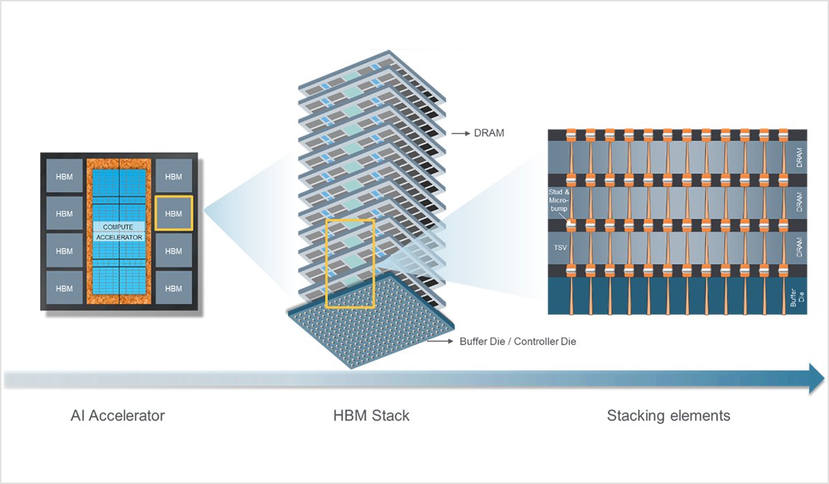
Focusing in on a specific type of DRAM that is the workhorse memory for AI today, Jinho An, Account Technologist Director, described the materials engineering steps needed to make HBM chips. Connecting the dies vertically adds nearly 20 additional front-end materials steps that rely heavily on Applied’s industry leadership in front-end wiring technologies. While the stacked dies are currently connected using micro-bumps, in the coming years we expect to see HBM adopting a more advanced technology called hybrid bonding, which directly connects chips to each other.
Finally, Sarah Wozny, Director of Heterogeneous Integration, discussed the advanced packaging roadmap. The only way to get all the transistors and on-chip memory we need for AI is to shift from system-on-a-chip to system-in-a-package. Sarah summarized three main drivers of the advanced packaging roadmap: stacking more chips vertically, shrinking the interconnects between the chips, and accommodating more chips with larger substrates called panels.

Clockwise from top-left: Mehul Naik, Sony Varghese, Sarah Wozny, Jinho An of Applied Materials
At Applied, we have been working on our AI-enablement strategy for a number of years. When we first introduced this playbook at our AI Design Forum in 2018, we talked about the goal of helping customers generate a 1,000X increase in performance-per-watt. Today, we believe this figure will be closer to 10,000X by 2040, leveraging the broad range of new materials, 3D structures, and advanced packaging technologies our team highlighted at SEMICON West 2024. Applied is co-innovating the inflection roadmap with our customers and it’s exciting to see the progress we are all making together.
Kevin Moraes
Vice President, Products and Marketing - Semiconductor Products Group

Kevin Moraes is Vice President of Products and Marketing in the Semiconductor Products Group at Applied Materials, Inc. He joined Applied in 2000 and holds a bachelor’s degree in chemical engineering from Annamalai University, an MBA from the University of California-Berkeley and a Ph.D. in materials science and engineering from Rensselaer Polytechnic Institute.
Beyond Backside Power: Scaling Chips to 2nm and Beyond Also Requires Frontside Wiring Innovations
Today’s advanced logic chips have as many as 20 layers of metal that support two types of wires – thin signal wires that switch transistors on and off, and thicker power wires that deliver the current that flows when the transistor is switched on. In the near future, all of the world’s leading chipmakers plan to move the power lines to the backside of the wafer, which promises to reduce wiring complexity, free up space for more transistors, and improve chip performance and power efficiency.
Power-Hungry AI Applications Demand More Energy-Efficient Computing
The computing industry’s relentless pursuit of more capable artificial intelligence is triggering the need for major inflections in logic and memory. While data center AI is expected to eclipse PCs and then smartphones as the number one driver of leading-edge foundry-logic and DRAM wafer starts, the growth of AI may be gated by the limits of the power grid – and push carbon neutrality goals years into the future – unless we dramatically improve the efficiency of chips and systems.

HBM: Materials Innovation Propels High-Bandwidth Memory Into the AI Era
Nvidia’s CEO Jensen Huang famously referred to the launch of OpenAI’s ChatGPT as an “iPhone moment” for artificial intelligence, describing it as “one of the greatest things that has ever been done for computing.”
